
World’s highest output X-band power amplifier for long-range wireless communication and radar
Higher quality protective film of GaN-HEMT improved power density for the first time in 20 years
March 25, 2024
Japanese Fabrication of GaN-HEMT
We live in a vibrant, convenient, safe and secure world, with huge numbers of electronic devices utilizing invisible radio waves in the background. Wireless communications, such as smartphones and Wi-Fi, weather and defense radars, are all essential to modern society. However, these devices rely on extremely high output power amplifiers for transmitting radio waves in order to increase communication and detection distances.
Fujitsu’s R&D teams have achieved an important new milestone, creating the world’s highest output X-band power amplifier for long-range wireless communication and radar.
This has been realized by improving the quality of the insulating protective film used in high electron mobility transistors (HEMTs) based on gallium nitride (GaN) material. GaN-HEMTs feature a wide bandgap and a robust structure, and are used for power amplifiers in the frequency range of X-band, which is widely used in wireless communications and radar. The result is a world-leading power density of 31 W/mm (watts per millimeter*). This is the highest value** for solid-state electron devices including GaN materials, and the first update to the top data in nearly 20 years.
・The detail of this technology are published in the academic journal “IEEE Electron devices letters”.![]()
- *Output power per 1 mm gate width in the transistor
- **Based on our company survey
Challenges to Overcome
To enhance output in a power amplifier, it is necessary to increasing both the current and operating voltage. For this reason, Fujitsu has actively proposed indium aluminum gallium nitride (InAlGaN), an alternative to conventional aluminum gallium nitride (AlGaN), as a potential candidate for achieving properties of both large current and high voltage, using an electron-generating layer called an electron supply layer or barrier layer in GaN-based HEMTs (Fig. 1). However, there have been historical issues with the use of InAlGaN material as a result of the degradation of the semiconductor surface due to the weak bonding of the constituent elements, In (indium) and N (nitrogen).
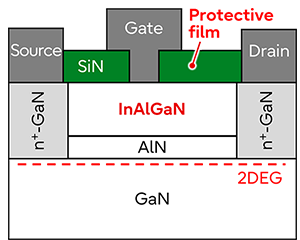 Fig.1 Schematic cross-sectional view of HEMT using InAlGaN
Developed Technology
In this study, we applied silicon nitride (SiN) formed by a method called thermal chemical vapor deposition (CVD), in which thin films are deposited by thermal decomposition products or chemical reactions, as a protective film on the surface of a semiconductor. Compared to the widely used plasma-enhanced CVD method, the thermal CVD method does not use a plasma containing a large amount of charged particles, which can cause the underlying material to deteriorate. Therefore, the degradation of the semiconductor surface can be greatly suppressed (Fig. 2). By applying the SiN film formed by the thermal CVD method to the InAlGaN-based HEMT, we were able to achieve both a further increase in the current value, a decrease in the electron trap caused by the current collapse, and an increase in the breakdown voltage. As a result, we successfully obtained a power density of 31 W/mm at an operating voltage as high as 90 V as an X-band power amplifier (Fig. 3 and 4).
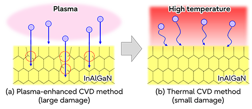 Fig.2 Differences in damage caused by deposition methods
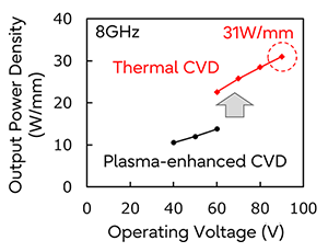 Fig.3 Improvement of power density by applying thermal CVD method
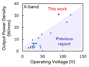 Fig.4 Benchmarks of X-band power amplifiers
Looking Ahead
In the future, we will be concentrating on improving the efficiency of this technology, with the aim of commercializing this technology. We are also planning to implement it in modules, and evaluate its reliability.
Related links
・Fujitsu Honored with IEEE Milestone for High Electron Mobility Transistor [Fujitsu Global Site](December 18, 2019, Press Release)
・Fujitsu Develops the World's Most Efficient Power-Saving Microwave Power Amplifier [Fujitsu Global Site](March 2, 2021, Topics)
・Towards 6G high-speed communications –Fujitsu develops the world’s most efficient J-band power amplifier(February 27, 2023, Topics)
・Successful beam control by sub-terahertz band array antenna for 6G high-speed communication(February 22, 2024, TECH BLOG)
For more information on this topic
Devices & Materials Research Center, Fujitsu Research
contact-gan@cs.jp.fujitsu.com
Share
Recommend
Connect with Fujitsu Research


