
Towards 6G high-speed communications –
Fujitsu develops the world’s most efficient
J-band power amplifier
Fujitsu’s solution achieves high output power and power saving, applying a MOS structure in InP-based HEMTs, in which electrons can move at high speed.
February 27, 2023
Japanese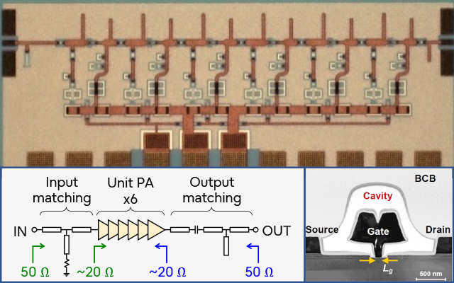 J-Band amplifier circuit and
InP-based HEMT cross section
Society is digitizing at a rapidly accelerating rate, with an ever-greater number of devices connecting to the Internet, moving beyond smartphones to automobiles, robots, and other devices in the future. The volume of data handled has also been increasing substantially, such as 4K/8K video, together with the total communication volume. In order to exchange this enormous amount of information efficiently without stress, the speed of wireless communication has to increase incrementally as well. There are also other considerations to take into account, in particular the need to control electricity consumption, in order to protect the global environment and realize a sustainable society. These are the drivers behind the 6th-generation mobile communication system (hereinafter 6G), which is the essential component for realizing high-speed wireless communications that will greatly exceed the current 5G with low power consumption, and using the sub-terahertz range that can utilize a wide bandwidth are attracting considerable attention.
At Fujitsu, we have succeeded in developing a new generation of power amplifier, which transmits with the highest power conversion efficiency in the world. As a result, it can reduce the power consumption of base stations in the sub-terahertz range, which is a candidate for high-speed wireless communication. We have been working on the development of high electron mobility transistors (HEMTs), using indium phosphide (InP)-based material with high electron mobility, and have succeeded in amplifying the signal at an extremely high frequency, called the J-band (220-325 GHz), by improving the quality of the insulating film.
The power amplifier using this transistor has also achieved the world's highest* power efficiency of 7%. As a result, HEMTs using InP materials are expected to become a candidate for realizing 6G communications.
This work was partially supported by “The research and development project for the expansion of radio spectrum resources (JPJ000254)” of the Ministry of Internal Affairs and Communication, Japan.
* Based on our company survey
Challenges to Overcome
New communication systems called Beyond 5G and 6G are required in order to realize the level of high-speed wireless communication that greatly exceeds the current 5G performance. The use of sub-terahertz waves, which are frequencies over 100 GHz, are being studied for this reason. We focused on the 300 GHz band, which is expected to have a particularly wide frequency allocation.
At extremely high frequencies such as sub-terahertz waves, the problem is that the radio wave reach distance is short. This is due to the large amount of atmospheric attenuation, as well as the difficulty in amplifying the signal as it approaches the operating limits of semiconductor devices. In addition, the higher the frequency, the less efficient the conversion of the applied power into signal amplification, resulting in increased power consumption. Therefore, in order to utilize sub-terahertz waves, it is necessary to achieve both high output and high efficiency of power amplifiers.
Fujitsu’s Breakthrough Technology
Our approach to solving these challenges was to develop J-band power amplifier devices and integrated circuits using InP-based HEMTs. As part of developing these new HEMT devices, we were able to improve the quality of aluminum oxide insulating films by applying a technique called "steam annealing", which enables a reduction of impurities and densification. By inserting this film as a gate insulator with an extremely thin film of 2 nm (nanometer), we were able to reduce current leakage and obtain good high-frequency characteristics over a wide gate voltage range (Fig. 1, 2).
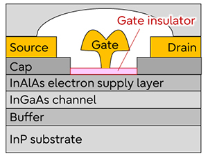 Fig.1 Schematic cross section of InP-based MOS-HEMT
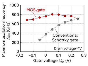 Fig.2 High-frequency characteristics of HEMTs
We have also developed a 6-stage HEMT integrated circuit (Fig. 3), which has an output power of 11 mW and the world's highest power-added efficiency of 7% (Fig. 4).
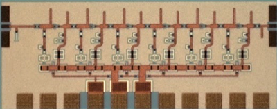 Fig.3 Photograph of J-band power amplifier chip
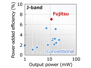 Fig.4 Benchmarks
** Patent pending
Looking Ahead
Fujitsu will continue to focus on improving the output and efficiency of power amplifier and conduct transmission experiments, working continuously towards the realization of practical applications for 6G in the future.
Related links
・Fujitsu Honored with IEEE Milestone for High Electron Mobility Transistor [Fujitsu Global Site] (December 18, 2019, Press Releases)
・Fujitsu Develops the World's Most Efficient Power-Saving Microwave Power Amplifier [Fujitsu Global Site] (March 2, 2021, Technical Topics)
For more information on this topic
Wireless Product Development Division, Mobile System Business Unit
Devices & Materials Research Center, Research Unit
Share
Recommend
Connect with Fujitsu Research


