
Fujitsu Develops the World's Most Efficient Power-Saving Microwave Power Amplifier
High Efficiency GaN-HEMT Reduces Energy Loss by 25%, supporting a Sustainable Society
March 2, 2021
Japanese Measurement of GaN-HEMT
A recent breakthrough from Fujitsu involves the development of the world’s most power efficient high gallium nitride (GaN) high electron mobility transistor (HEMT) power amplifier. Thanks to Fujitsu’s cutting edge technologies, it is now possible to reduce the power consumption of various radio frequency (RF) applications.
Fujitsu’s newly developed technology enables a semiconductor crystal layer for GaN-HEMT to be fabricated on an unconventional high-quality GaN substrate. By reducing defects and impurities in the semiconductor crystal layer, GaN-HEMTs’ efficiency has been significantly improved, achieving the world's highest power conversion efficiency of 82.8% at a frequency of 2.45 GHz, the frequency most widely used in wireless LANs, industrial, scientific, and medical fields. This new method reduces power amplifiers’ overall energy loss by some 25%, compared with existing technology, and will have multiple benefits for RF applications. Fujitsu’s development will enable a significant power consumption reduction for future RF applications used in evolving sensing devices and networks.
Details of this technology have been published in the journal "Applied Physics Express".
https://iopscience.iop.org/article/10.35848/1882-0786/abc1cc/meta![]()
Background
Our lives today are made all the more convenient thanks to the wide variety of devices that use radio waves, in which many electronic components play an integral part. But this convenience comes at a price – namely the potential for large amounts of energy loss due to the challenges of using electric power 100% effectively. This energy loss tends to increase as the frequency of radio waves rises. For example, power amplifiers that amplify electrical signals such as microwaves and millimeter waves (used in radar and radio communications), are relatively inefficient, operating typically at between 30-70%. In the future, the volume of data traffic in wireless communications is rapidly expected to grow, reaching around 80 times the current level by 2030. In turn, this will involve using higher frequencies in order to improve communication capacity, as well as to enhance radar resolution. The overall power consumption of equipment is likely to increase significantly in this new era, as the efficiency of power amplifiers degrades further. This is the background to the requirement for a new generation of power amplifiers, capable of much higher power conversion efficiency, as we work towards realizing a more sustainable society with consideration for the global environment.
Challenges
With conventional GaN-HEMT power amplifiers, the semiconductor crystal layer (GaN epitaxial layer) is generally formed on a heterogeneous substrate, such as silicon carbide (SiC) or silicon (Si). The issue is that GaN epitaxial layers on heterogeneous substrates contain a large number of crystal defects. These defects trap electrons traveling in the GaN epitaxial layer during a power amplifier’s high voltage operation, which causes a deterioration of current in the HEMT (Fig. 1). As a result, the output power and the power conversion efficiency of the GaN power amplifier are degraded.
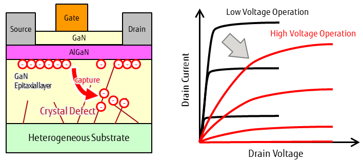 Figure 1 Electron Capture by Crystal Defects in Conventional GaN-HEMTs and Their Effects
Fujitsu’s Breakthrough Technology
To address this challenge, we focused on developing GaN-HEMTs with a higher efficiency than conventional transistors, by not only using a high-quality GaN substrate but also applying a treatment to the GaN substrate surface before the crystal epitaxial grows.
This new high-quality GaN substrate has a uniform crystal lattice spacing between the substrate and epitaxial layers, with GaN epitaxial layers grown on this having significantly fewer crystal defects. In fact, the defects are reduced by more than two orders of magnitude compared with conventional substrates in which each crystal lattice spacing is different (Fig. 2).
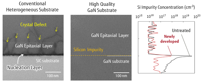 Figure 2 Comparison of Cross-Sectional Images of GaN Crystals and Comparison of Si
Impurity Concentrations at the Epitaxial Layer/GaN Substrate Interface in High-Quality Substrates
However, as this method involves a high-quality crystal with very few crystal defects, even very subtle Si impurities remaining on the surface of the GaN substrate can degrade the electrical characteristics of the epitaxial layer. Specifically, when silicon impurities are incorporated into the epitaxial layer and activated, a highly conductive layer is formed near the substrate interface. This causes leakage during high-frequency operation, and can hinder efficiency improvement as result.
Our technique is designed to improve the efficiency of GaN-HEMTs by deactivating the Si impurities. We achieve this by lowering the concentration of Si compared to the concentration of iron (Fe) added to inactivate the GaN substrate (2-9 x 1018 cm-3), and applying a special treatment to the surface of the GaN substrate before epitaxial growth. As shown in Fig. 3, in a conventional GaN-HEMT power amplifier without any surface treatment of the GaN substrate, the leakage of high-frequency signals increases as the frequency rises from 1 GHz to 10 GHz. However, by applying our new technique, the leakage of high-frequency signals can be suppressed regardless of the frequency.
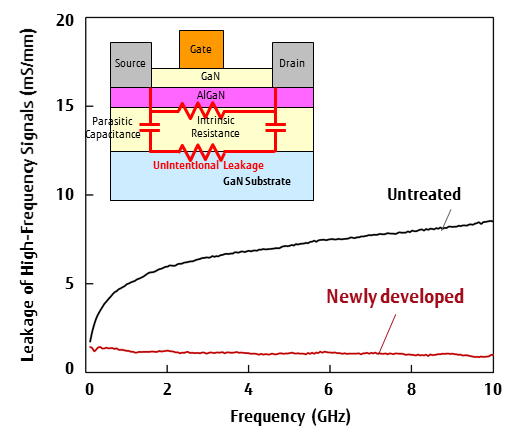 Figure 3 Comparison of Leakage of High-Frequency Signals in Prototype GaN-HEMTs
Evaluating the output characteristics at 2.45 GHz of the newly developed GaN-HEMT power amplifier, we were able to demonstrate 82.8% efficiency performance, which is currently the world's highest efficiency in the 2-3 GHz band (Fig. 4).
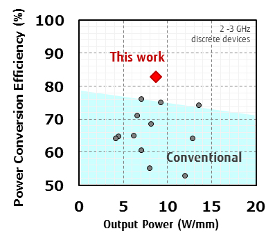 Figure 4 Comparison of the Power Characteristics of Fujitsu’s Newly Developed Technology
We believe that this technology will play a major part in helping to achieve a more sustainable society by reducing the power consumption associated with the growing number of RF applications, such as wireless networks, sensing devices and industrial heating devices, and consequently reducing CO2 emissions. In addition, the improved operation of these devices, with less heat generation, will also enable cooling mechanisms for RF applications to be further miniaturized. Fujitsu is committed to continuing our research and development of high-efficiency power amplifiers, achieving higher frequencies as well as reducing the power consumption of future devices using radio waves.
This research was partly supported by the Japan Ministry of the Environment, under the Technical Innovation to Create a Future Ideal Society and Lifestyle project.
An Inside View from the Development Team:
Yusuke Kumazaki, Researcher, Advanced Materials Project, Device & Materials Research Center
"We greatly appreciate the Japan Ministry of the Environment’s support for this project, as well as the terrific cooperation between our research group members. It is very rewarding to have achieved our challenging goal of improving the efficiency of power amplifiers. In the future, we will be concentrating on demonstrating the outstanding performance of the technology developed through this project, as we work towards the realization of a future decarbonized society."
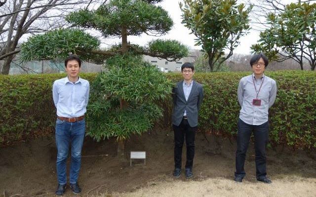 Development team: From left to right: Junji Kotani project manager, Yusuke Kumazaki researcher, Shirou Ozaki researcher
Inquiries regarding this matter
Please note that we would like to ask the people who reside in EEA (European Economic Area) to contact us at the following address.
Ask Fujitsu
Tel: +44-12-3579-7711
http://www.fujitsu.com/uk/contact/index.html![]()
Fujitsu, London Office
Address :22 Baker Street
London United Kingdom
W1U 3BW
Share
Recommend
Connect with Fujitsu Research


