When I was four years old, my parents gave me an illustrated book as a gift. Each section of the book was organized by theme, such as flowers, insects, and stars. The one I liked best was the one on stars. It depicted beautiful planets, and I became captivated, reading it repeatedly with fascination.
Influenced by books I read in my childhood, I specialized in fundamental research during my university years on the behavior of materials under ultra-high pressure. By simulating phenomena that occur at the center of the earth and investigating the properties of materials and changes caused by pressure, I felt that this research would be useful for my understanding of what triggers earthquakes and other phenomena. As part of my research, I also conducted an experiment in which I prepared two diamonds, the hardest materials on earth, and observed their behavior by applying ultra-high pressure from the upper and lower sides of the sample.
It was during my graduate school years that I began to develop an interest in practical technologies that are useful to society. Using the synchrotron radiation facility SPring-8 accelerator, I was involved in research to improve the performance of dielectrics for future USB memory sticks. Although this research did not produce immediate practical results, it served as a catalyst for confirming my desire to develop technologies that contribute to society.
Since joining Fujitsu, I have been involved in many projects, but one that left a particularly strong impression on me was the development of a high-power amplifier using aluminum nitride (AlN) (*1). AlN is a technology that was expected dramatically to increase wireless communication and radar detection distances. Especially in regions with many islands, it is difficult to build a wireless communication base station on each island due to environmental constraints. With this technology, a single base station can provide communications to the surrounding islands.
At that time, we faced a challenge related to the leakage current of the transistors we produced. The leakage current, which is an undesired current that occurs in electronic circuits and is supposed to be suppressed, was proving difficult to lower. If the leakage current is not lowered, it hinders the proper functioning of the transistors, preventing them from exhibiting their power characteristics. As a result, the wireless communication transmission range and the radar detection range of radar was impacted and could not reach the expected distances.
To identify the root cause, we conducted numerous investigations and verifications, leading to many frustrating days of persistent struggle. One day, while observing the current paths using an electron microscope, we discovered the reason behind the inability to reduce leakage current. The transistor, composed of multiple electrodes, typically consists of three components: the source electrode, gate electrode, and drain electrode. However, it was found that elements that should have been structurally separated were, in fact, electrically connected. This phenomenon led to the occurrence of the problem.
After examining details at the nanometer scale, it was revealed that oxygen was causing the connection between the gate electrode and the drain electrode. Therefore, we attempted to lower the leakage current by including nitrogen in the film. To suppress the leakage current effectively by incorporating nitrogen, it was necessary to find the optimal ratio of nitrogen. Through repeated trial and error, we discovered that a ratio of less than 1% was the optimal solution, successfully reducing the leakage current. Sheer persistence and a refusal not to give up ultimately led to our being able to solve the challenge, contributing to the development of AlN technology that can dramatically increase the wireless communication and radar detection distance.
I believe that actively engaging in hands-on work is crucial in R&D. In the current research I am undertaking, it is essential to create samples of materials and evaluate them personally. The Fujitsu Research at Atsugi area, where I am currently based, is well-equipped with devices for both material synthesis and evaluation. This has contributed to a highly efficient and smooth progression of the R&D process.
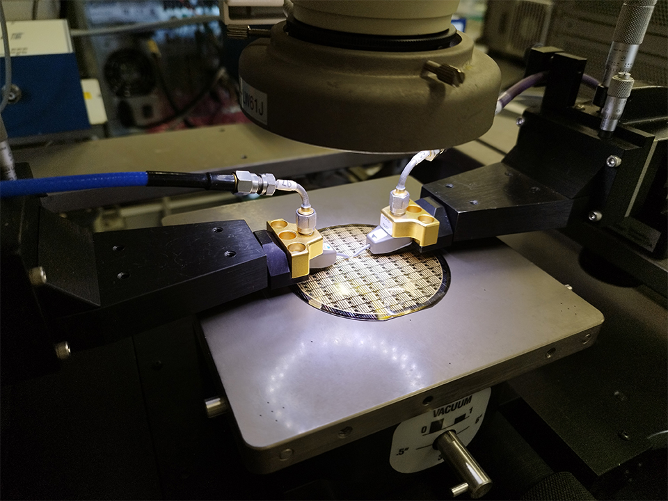
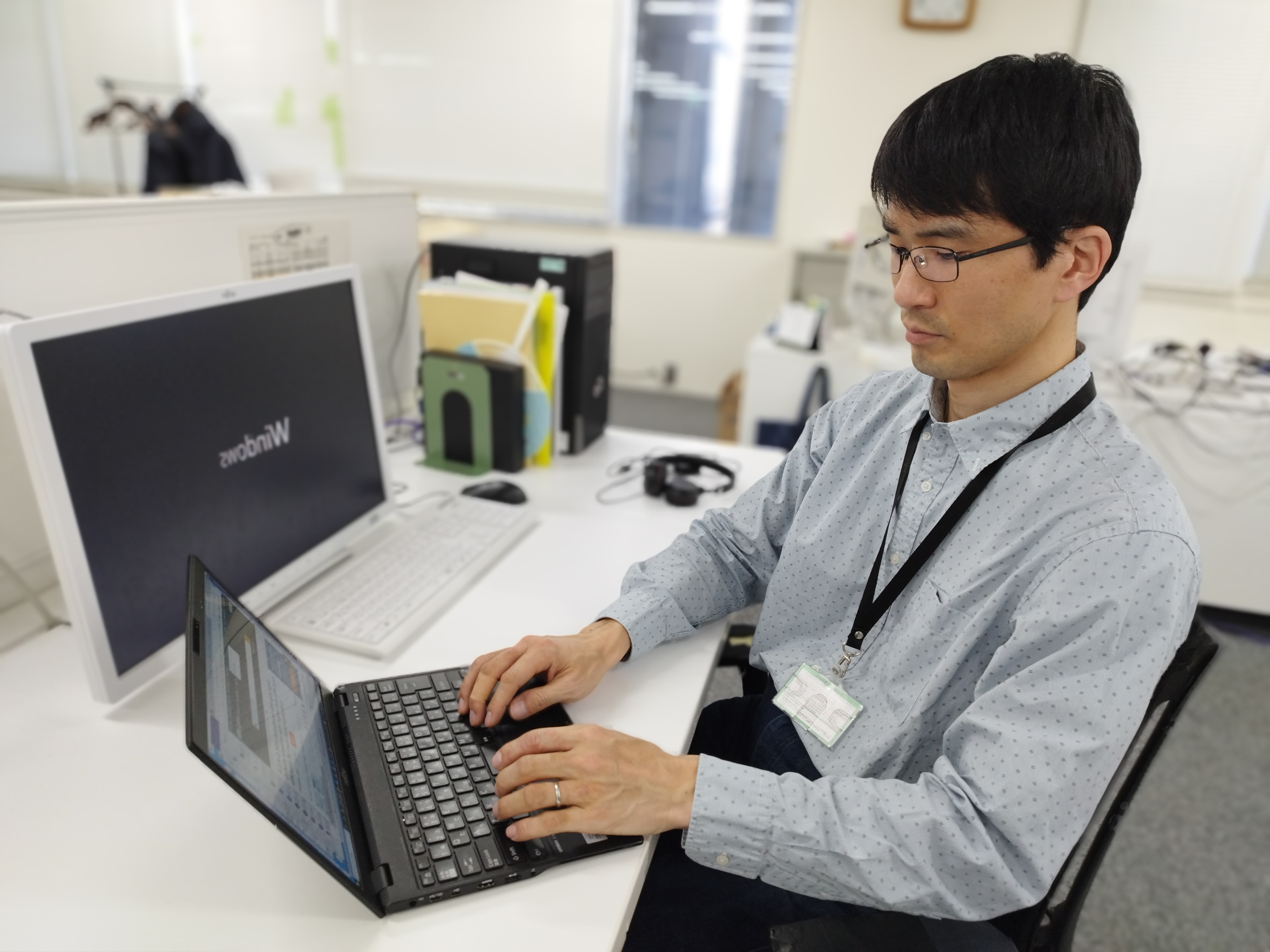
During the sample evalution of GaN-HEMT (gallium nitride high electron mobility transistor)
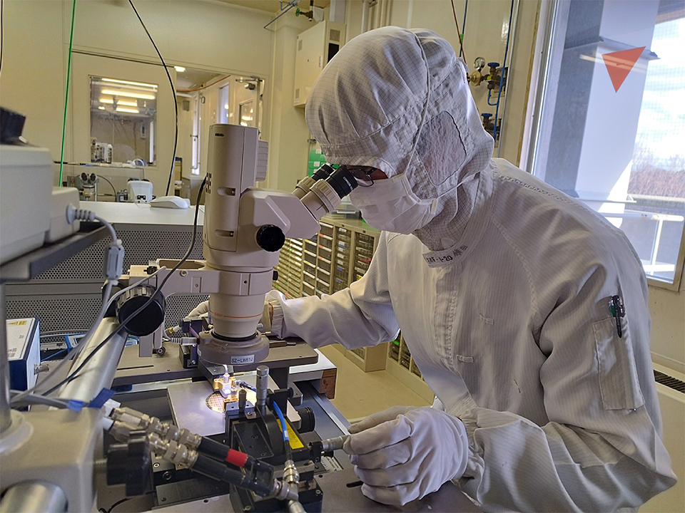
Sample evaluation of GaN-HEMT in the clean room at Fujitsu Research at Atsugi, Japan.
I aspire to be a pioneer in new technology by maximizing the characteristics of transistors in circuit design. Even if individual transistors are optimized for performance, their capabilities cannot be fully realized if they do not suit communication devices or signal processing equipment. Therefore, it is essential to design circuits that meet the requirements of such devices and optimize the entire system to make it operational. Therefore, my aim is to focus on circuit design for communication applications.
In current wireless communication, multiple base stations are primarily erected to cover various frequency bands. In particular, it is difficult to cover the entire frequency band from 2 GHz to 4 GHz with a single base station. We are seeking a solution to cover a wider frequency band with a single base station by updating the technology to maximize the transistor characteristics(*2). My objective is to contribute to Fujitsu, hoping the company will lead the market by offering products that can cover a wide range of frequency bands.
My daily routine is to wake up in the quiet early morning and having a leisurely breakfast. This gives me a really good start to the day. To stay healthy, I also refresh my mind and body with a weekly running session. I regularly participate in running events, and the sense of accomplishment upon completing them is truly fulfilling.
I am currently engaged in R&D with a certain degree of freedom in accordance with my research theme. This requires making choices and decisions on my own, accompanied by responsibilities, but I consider it necessary and find it fulfilling. If there are those who are interested in our research, I would be delighted to engage in discussions and encourage us to develop together at Fujitsu.


