
Supercomputer Fugaku CPU A64FX Realizing High Performance, High-Density Packaging, and Low Power Consumption
Release date: November 11, 2020
The A64FX was developed as a processor for the supercomputer Fugaku. For the semiconductors, the 7- nm CMOS process technology of TSMC [1] has been used. For higher density, the Tofu interconnect D and the PCI Express controllers have been implemented in the CPU chip, and the high-bandwidth 3D stacked memory is integrated in the package.
The A64FX employs the Arm architecture to improve the software development environment while inheriting Fujitsu’s proven high-performance microarchitecture. In addition, we worked on the specification of Scalable Vector Extension (SVE) as a lead partner of Arm Limited, the result of which has been adopted.
This article outlines the A64FX and describes its high-performance microarchitecture, architecture to achieve high-density packaging, and low power consumption design.
- 1. Introduction
- 2. A64FX overview and adoption of Arm architecture
- 3. High-performance microarchitecture
- 4. High-density architecture
- 5. Low power consumption design
- 6. Conclusion
1. Introduction
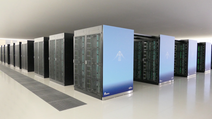
The A64FX (Figure 1) was developed as a processor for the supercomputer Fugaku (hereafter, Fugaku). Fugaku features 158,976 processors [2]. These processors require high performance, high-density packaging, and low power consumption, all at high levels. The software development environment is also important.
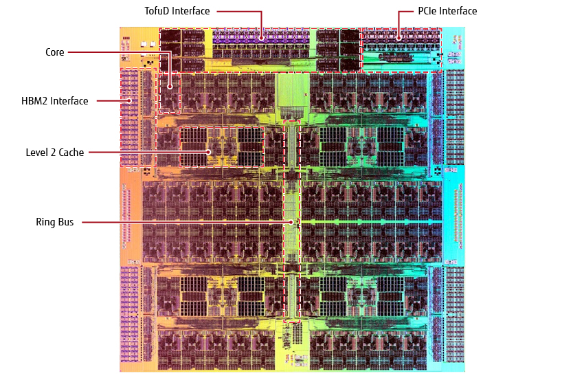
Figure 1 Die photo of A64FX CPU.
This article outlines the A64FX and describes its high-performance microarchitecture, architecture to achieve high-density packaging, and low power consumption design.
2. A64FX overview and adoption of Arm architecture
For the A64FX, we decided to work on development with the aim of achieving the capability of higher-speed application execution based on the microarchitectures of processors developed by Fujitsu up to now, including the processor of the K computer.
In order to accelerate application performance, we analyzed various applications and optimized the entire processor, revising the configuration of various blocks, optimizing resources, adding new circuits, selecting and optimizing memory components, and optimizing OS operations. In addition, we implemented measures to save power across a wide range of levels from the architecture to the device level with the aim of providing a system that uses the A64FX, a general-purpose CPU, with the capability of achieving performance per power equivalent to that of a system equipped with a GPU.
Figure 2 shows a block diagram of the A64FX CPU [3]. There are four core memory groups (CMGs), each of which is composed of 13 cores (12 used as computing cores and one as an assistant core), level 2 cache and memory controller, and a ring bus network on a chip (NoC) is used to connect them with the Tofu Interconnect D (hereafter, TofuD) [4] interface and PCI Express (PCIe) interface.
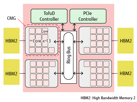
Figure 2 Block diagram of A64FX CPU.
In developing the A64FX, the Arm architecture was adopted with the aim of having the supercomputer Fugaku accepted by a wider range of software developers than the K computer, which saw a full-scale launch in 2012, and putting in place an environment allowing use of the latest software. The Arm architecture is an instruction set developed by Arm Limited (hereafter, Arm) widely used in software development for smartphones and embedded devices. Recently, Arm processors for servers have appeared by extension to a 64-bit architecture, which is the standard in the server sector, and new addition of the hypervisor extension feature for servers. These developments have raised expectations for expansion of Arm into the server sector.
In offering the Arm architecture as a processor for high-performance computing (HPC), single instruction, multiple data (SIMD) extension, a unique feature of the Arm architecture, became an issue. This SIMD extension, known as the Advanced SIMD, is used for accelerating media processing and digital signal processing (DSP) for embedding and other applications. The SIMD length is 128 bits, the same as the K computer. This is shorter than 256 bits and 512 bits, the current trends for HPC CPUs, and was unsuitable for improving the computing performance per core. In addition, based on Fujitsu’s past experience in HPC development, instructions useful for the HPC applications were also insufficient.
Therefore, by collaborating with Arm, Fujitsu contributed as a lead partner to the specification of Scalable Vector Extension (SVE) capable of high-speed execution of HPC applications including scientific computing and AI, the result of which has been adopted for the A64FX.
3. High-performance microarchitecture
With the A64FX, microarchitecture exclusively for Fugaku was developed with the aim of speeding up the execution of user applications. This section outlines the microarchitecture and describes the elemental technology utilized to make it a reality.
3.1 Microarchitecture overview
Figure 3 shows the pipeline of the A64FX [3]. A core is composed of the instruction control unit, execution unit, and level 1 cache unit. The instruction control unit performs instruction fetch, instruction decode, instruction out-of-order processing control, and instruction completion control.
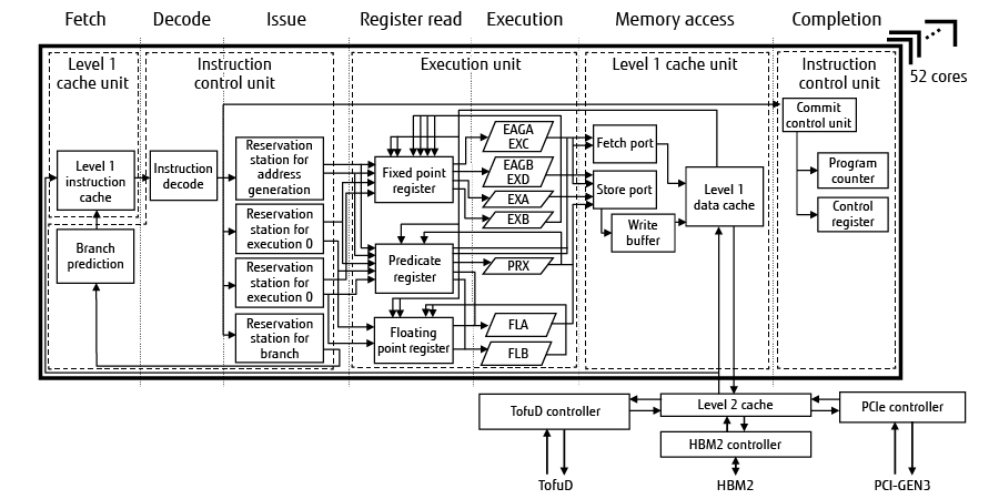
Figure 3 Diagram of A64FX pipeline.
The execution unit is equipped with two fixed-point functional units (EXA/EXB), two functional units for address computation and simple fixed-point arithmetic (known as EAGA/EAGB for address calculation and EXC/EXD for fixed-point arithmetic), two floating-point units for executing SVE instructions (FLA/FLB), and one predicate unit for executing predicate arithmetic (PRX). Both floating-point units have a 512-bit SIMD configuration and can perform a floating-point multiply-accumulate operation every cycle. Therefore, each computing core is capable of 32 double-precision floating-point operations per cycle and use of all computing cores in the chip allows 1,536 double-precision floating-point operations to be performed per cycle. With single-precision floating-point operations and half-precision floating-point operations, the number of operations that can be performed is twice and four times the number of double-precision floating-point operations, respectively. It operates at 1.8 GHz/2 GHz/2.2 GHz, although the operating frequency varies depending on the system in which it is installed.
The level 1 cache unit processes load/store instructions. Each core has a 64-KiB instruction cache and a 64-KiB data cache. The data cache is configured to be capable of two simultaneous load accesses and executes two 64-byte SIMD loads or one 64-byte SIMD store.
The level 2 cache unit has 8 MiB of unified cache per CMG and is shared by 13 cores including the assistant core.
3.2 Proven microarchitecture and resource optimization
For the A64FX, we have implemented various types of hardware resource optimization based on the high-performance, high-reliability microarchitecture adopted in mainframe, and UNIX servers, and the K computer, which Fujitsu previously developed.
In particular, for the numbers of reorder buffer (ROB), reservation station, and other queues, which are important as performance indicators, we have adopted control to accelerate the release by judging the release timing of the queue at the time of instruction execution. This ensures the instruction execution performance without unnecessarily increasing the number of queue entries, which reduces the chip area by curbing the increase of logic circuits.
3.3 Branch prediction circuits
We have employed several branch prediction circuits so that optimum branch prediction can be performed with various applications.
For example, we have employed a circuit that uses a piecewise linear algorithm to perform branch prediction. This allows for high-accuracy branch prediction capability even with a program that has a complicated instruction structure. As a result, it is possible to perform branch prediction based on an instruction execution history for a long time, and high prediction accuracy can be realized.
We have also adopted a circuit capable of branch prediction by detecting a simple loop or other program structure. By buffering the loop instruction sequence while the program is looping, operation of the instruction fetch unit and other branch prediction circuits is stopped to reduce power.
3.4 Virtual fetch/store port circuit
A fetch/store port used in load/store instructions is a queue located in the later stage of the pipeline. Therefore, several cycles are required from the release notification to the decoder unit that manages the resource to the actual use of the released entries. When the resource is full, decoding of instructions including those that do not use the fetch/store port stops and some measures were required to deal with SVE instructions, which use many fetch/store ports.
To resolve this issue, we decided to provide the A64FX with the support of the virtual fetch/store port function to improve the use efficiency of fetch/store ports with the minimum circuit scale for improving performance.
Previously, the instruction decoder was used for fetch/store port resource management. With the A64FX, however, we have allocated a larger number of virtual fetch/store ports than that of the actual fetch/store ports for the instruction decoder and assigned resource management of the fetch/store ports to the reservation station used for load/store-based instructions. This prevents instruction decoding from being stopped even when all fetch/store ports are in use, which has proved to provide an effect equivalent to increasing the number of fetch/store port entries.
3.5 Level 1 data cache to support various access patterns
In order to maximize the efficiency of 512-bit SIMD, it is important to maintain the access throughput of the L1 data cache in load instructions that transfer data to registers. When load instructions with addresses not on 512-bit boundaries are sequentially executed in the order of address, access across cache lines occurs once in several instructions. To avoid performance degradation in this case, the L1 data cache of the A64FX is configured to allow each of the two lead ports to always access two consecutive cache lines. Thus, even when a load instruction accesses across a cache line, a throughput of 512 bits x 2 is maintained every cycle.
3.6 Accelerate throughput performance of gather-load instruction
A gather-load instruction reads discontinuous multiple-element data from the memory and writes it to one register. Although the data are discontinuous, with HPC applications, it has been made clear that data have locality, as in multiple elements accessing close addresses. Based on this feature, a accelerate mechanism called combined gather has been employed for the A64FX. The combined gather mechanism disassembles a gather-load instruction into groups of two elements instead of processing the elements one by one. When the elements belonging to the same group access the memory within the same 128-byte boundary, the process is completed by one cache access. As a result, double throughput performance has been realized in comparison with processing one element at a time.
3.7 Prefetch mechanism
Accessing the main storage and a lower-level cache requires a significant amount of time and. To improve the program performance, prefetching is important to hide the access time. Methods of realizing prefetching can be roughly classified into software-based and hardware-based methods.
1) Software prefetch
The A64FX supports the SVE contiguous prefetch instruction and the SVE gather prefetch instruction of SVE in addition to the ARMv8 prefetch instruction, the normal prefetch instruction. As a result, a prefetch over multiple cache lines is also issued by one instruction.
2) Hardware prefetch
The hardware prefetch mechanism of the A64FX has two modes: the stream detect mode and the prefetch injection mode.
In the stream detect mode, prefetches are issued for sequential access. It uses a special mechanism called a prefetch queue to monitor memory access and, when a sequential access stream is detected, prefetches are issued in the direction of the address sequence.
In the prefetch injection mode, prefetches are issued for addresses at a certain distance from the memory access. Programs using this mode can issue prefetches for strided access to access addresses at a certain distance by setting information on prefetch addresses in advance in a dedicated prefetch control register.
4. High-density architecture
To achieve higher density, the A64FX—which is a system on a chip (SoC) integrating various controllers—has four high bandwidth memories (HBM2) in the package. Each of the four CMGs is connected to the respective HBM2 to ensure low latency and high bandwidth.
4.1 CMG configuration and ccNUMA
Figure 4 shows the CMG configuration and a connection diagram [5]. The CMG is composed of 13 cores, a level 2 cache shared by those cores, and a memory controller.
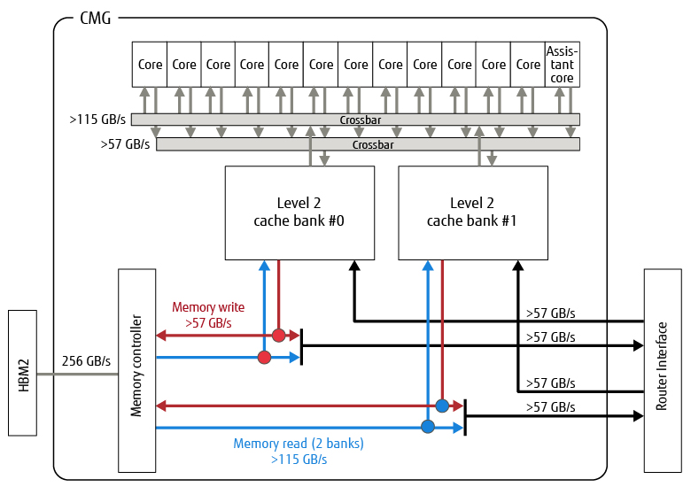
Figure 4 Diagram of CMG configuration and connection.
The capacity of the level 2 cache is 8 MiB per CMG, and two level 2 cache banks and 13 cores are connected by crossbars. The level 2 cache has a function to guarantee the cache coherence of the entire chip so that the software can treat the CMG as a non-uniform memory access (NUMA) node.
Cache coherence in the A64FX is centrally managed by a level 2 cache pipeline without using a general home agent mechanism. The level 2 cache pipeline consists of one pipeline: the first half is called the local pipeline and the second half the global pipeline. The directory information for managing cache coherence between CMGs is stored in a part called TAG Directory (TAGD) and accessed in the global pipeline. If coherence management closed in the CMG is possible, response to the cores is initiated at the end of the local pipeline and, if not, coherence management between CMGs is initiated at the end of the global pipeline that follows. This configuration reduces the hardware resources requirement and realizes a low-latency cache-coherent NUMA (ccNUMA) system.
4.2 SoC architecture
Figure 5 shows connections between CMGs [4]. Four CMGs, a TofuD/PCIe controller and an interrupt controller are connected by two ring buses and six ring stops. The A64FX also employs a proprietary NoC topology with CMG interconnect paths for connecting between adjacent CMGs. The throughput of the ring buses and CMG interconnect paths is more than 115 GB/s each.
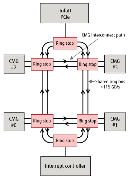
Figure 5 Diagram of connections between CMGs.
Provision of the CMG interconnect paths makes it possible to avoid the effect of use of ring buses due to data transfer with TofuD network and I/O, and interrupt requests from the interrupt controller, etc. It also realizes a configuration with a smaller number of connections between blocks than use of a crossbar, ensuring the throughput performance between adjacent CMGs.
4.3 HBM2 and memory controller
The A64FX uses HBM2, which is a 3D stacked memory with much higher bandwidth than DDR4 DIMMs used in general servers. The memory controller developed exclusively for HBM2 is housed in the processor and the CPU chip and HBM2 are integrated into a single package using the 2.5D packaging technology to ensure low latency and high memory bandwidth of 1,024 GB/s. With the memory controller developed exclusively for HBM2, we have optimized the control method to maximize the performance in accordance with the characteristics of HBM2 memory while ensuring strong reliability equivalent to that of a mainframe.
4.4 TofuD and PCIe controllers
As external input/output interfaces, the A64FX has a TofuD for realizing a massively parallel system by mutually connecting CPUs and a PCIe bus for connecting I/O devices. The TofuD has 20 lanes of high-speed serial signals of 28-Gbps transmission speed and interconnects up to 10 CPUs with a bandwidth of 6.8 GB/s. The PCIe has 16 lanes of high-speed serial signals of 8-Gbps transmission speed and the bandwidth is 16 GB/s.
Figure 6 shows a block diagram of TofuD. The TofuD has six network interfaces called TNIs and interconnects with 10 CPUs through a network router. The network of TofuD has a 6D mesh/torus topology as with the K computer [6-8].While the node address of the network is physically 6D, a user process is given virtual 3D coordinates to allow use of a conventional communication algorithm for 3D connection. As with the K computer, the communication function of the TofuD is also equipped with remote direct memory access (RDMA) communication and barrier-synchronized communication as the functions that can be used directly from a user process and system packet communication as the function used by the system for IP packet transfer. In terms of the types of RDMA communication, atomic read-modify-write, which is extended by Tofu2 [9] after the K computer, is supported in addition to put and get in the same way as with the K computer. The RDMA communication of Tofu has its own virtual storage and transfers data directly between the virtual address spaces of user processes managed by the OS of the respective nodes. Each data transfer is assigned a global process ID and is protected to refer only to processes executed by the same parallel program. In comparison with the conventional K computer and Tofu2, TofuD has a greater number of simultaneous communications and enhanced fault tolerance and barrier-synchronized communication. The following describes the respective enhancements.
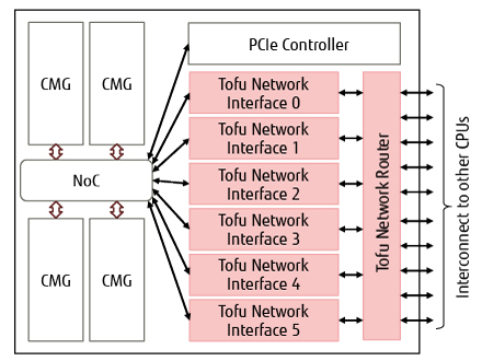
Figure 6 Block diagram of TofuD.
1) Roughly twice as much total communication bandwidth
Most collective communication algorithms optimized for 3D connections communicate simultaneously in six directions in three dimensions. However, the number of network interfaces was conventionally four and simultaneous communication was possible in only up to four directions. With TofuD, the number of network interfaces has been increased to six, which has allowed a communication algorithm to be used that realizes high bandwidth by simultaneously communicating in three directions in three dimensions. The total bandwidth of simultaneous communication has been enhanced from 20 GB/s with the K computer to 40.8 GB/s.
2) High fault tolerance
With the K computer, errors were detected for each link to the adjacent node and the data was retransmitted. In addition, a link with high error detection frequency was disconnected. With Tofu2, a link that was disconnected was subsequently automatically reconnected with the number of the lanes reduced to half. If the number was already reduced to half, the link was reconnected by using different lanes, but no means was implemented to automatically recover the number of lanes.
In contrast, TofuD has been equipped with a function for reducing the bandwidth when the error detection frequency is high and restoring the reduced bandwidth when the error detection frequency is reduced. Specifically, when the error detection frequency is high, the function transfers the same data by two lanes while maintaining the link to improve fault tolerance. And when the error detection frequency is low, it restores the mode of using the lanes to transfer different data to recover the bandwidth.
3) Six barrier-synchronized communications
Along with the introduction of CMGs, the number of resources for barrier-synchronized communication have been increased to expand the number of contraction operation elements. While one of the four network interfaces was conventionally used for barrier-synchronized communication, with TofuD, all six network interfaces perform barrier-synchronized communication. Conventionally, contraction operation was possible for one element per barrier synchronization, regardless of data type. But with TofuD, contraction operation is possible for eight integer elements or three floating point number elements.
5. Low power consumption design
In terms of low power consumption, measures have been taken to save power across a wide range of levels from the architecture level to the device level.
5.1 Architecture-level power saving
Most of the application operations can now be localized in a CMG by grouping the computing cores and directly connecting the memory to each group and by avoiding process mapping across groups. As a result, the average distance travelled by data is shortened, leading to reduced power.
5.2 Circuit-level power saving
In order to support 512-bit SIMD, the access method of the level 1 data cache was reviewed. Since throughput is more dominant than latency in the performance of applications that heavily use SVE vector load, SVE load instructions employ a scheme that can significantly reduce power when accessing the level 1 data cache by slightly increasing latency.
We also reviewed the data forwarding circuit in the arithmetic pipeline and added a circuit to reduce power consumption by reducing reference to the register file with large power consumption.
6. Conclusion
This article described the high performance, high-density packaging, and low power consumption design of the A64FX.
The A64FX was developed with the aim of significantly improving the performance per power of a wide range of applications. Fujitsu has moved ahead with co-design together with the RIKEN Center for Computational Science. Different teams for processor development, system development, software development, compiler development, and performance evaluation have collaborated closely to successfully develop new technologies, advance conventional technologies, and achieve the goal.
We expect that the supercomputer Fugaku will contribute to the resolution of issues in various fields in the future and that the A64FX will be accepted by a wide range of software developers to accelerate DX.
All company and product names mentioned herein are trademarks or registered trademarks of their respective owners.
References and Notes
- Taiwan Semiconductor Manufacturing Company, Ltd.Back to Body
- Y. Ajima et al.: The Tofu Interconnect D. IEEE International Conference on Cluster Computing, pp. 646–654 (2018).Back to Body
- S. Yamamura: A64FX High Performance CPU Design, Cool Chips 22 (2019).Back to Body
- Y. Ajima et al.: Tofu: A 6D Mesh/Torus Interconnect for Exascale Computers. IEEE Computer, Vol. 42, No. 11, pp. 36–40 (2009).Back to Body
- Y. Ajima et al.: The Tofu Interconnect. IEEE 19th Annual Symposium on High Performance Interconnects, pp. 87–94 (2011).Back to Body
- Y. Ajima et al.: The Tofu Interconnect 2. IEEE 22nd Annual Symposium on High Performance Interconnects, pp. 57–62 (2014).Back to Body
About the Authors

Mr. Okazaki is engaged in processor development.

Mr. Tabata is engaged in processor development.

Mr. Sakashita is engaged in processor development.
Mr. Kitamura is engaged in processor development.

Ms. Takagi is engaged in processor development.
Mr. Sakata is engaged in processor development.

Mr. Ishibashi is engaged in processor development.

Mr. Nakamura is engaged in processor development.

Dr. Ajima is engaged in architecture development.
Related Links
- Supercomputer Fugaku (Fujitsu innovation)

- FUJITSU Processor A64FX (Products)
- Fujitsu Employee Wins Medal of Honor with Purple Ribbon in the 2020 Spring Conferment for Inventing Technology for Supercomputers (Press releases)
- Fujitsu Presents Post-K CPU Specifications (Press releases)
- High-dimensional Interconnect Technology for the K Computer and the Supercomputer Fugaku (Fujitsu Technical Review)
- Taking on the challenge of COVID-19: The birth of six-dimensional interconnect technology for the supercomputer Fugaku Part1 (Fujitsu Blog)
- Taking on the challenge of COVID-19: The birth of six-dimensional interconnect technology for the supercomputer Fugaku Part2 (Fujitsu Blog)