Archived content
NOTE: this is an archived page and the content is likely to be out of date.
Fujitsu Laboratories and imec Holst Centre Develop Wireless Transceiver Technology for Medical Devices
Complies with the 400 MHz-band international standard while consuming 1/10th the power of previous models, lightening the burden on patients who use sensors
Fujitsu Laboratories Ltd.,imec Holst Centre
Kawasaki, Japan, and Eindhoven, The Netherlands, February 12, 2014
Fujitsu Laboratories Ltd. and imec Holst Centre today announced that they have developed a wireless transceiver circuit for use in body area networks (BAN) for medical applications that adheres to the 400 MHz-band international standard.
While the subject of high expectations for medical applications, wireless monitoring of brainwaves or other vital signs has in the past required over a dozen milliwatts (mW) of electric power. Now, however, by optimizing the architecture and circuitry, Fujitsu Laboratories and imec Holst Centre have succeeded in reducing the electric power requirements of wireless transceiver front-ends, to just 1.6 mW when receiving data and 1.8 mW when transmitting.
This technology extends by approximately ten-fold the battery life of conventional sensor products used for patient monitoring. This cuts the frequency of battery replacement or recharges, lightens the burden on patients, and increases the work efficiency of medical practitioners.
Based on this joint research into wireless transceiver technology, Fujitsu Laboratories plans to apply it to non-medical uses, as well, such as to the monitoring of societal infrastructure, thereby further enhancing network front-end interface technologies.
Details of this technology were announced at the IEEE International Solid-State Circuits Conference 2014 (ISSCC 2014), which opened February 9 in San Francisco (ISSCC Presentation 9.7)
Background
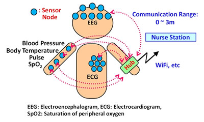
In the field of healthcare and medicine, BAN have attracted attention for their potential application in collecting patient-monitoring data via a wireless network of sensors placed on the patient's body (Figure 1). The various sensor nodes that make up the BAN all need battery power, and to make the system as convenient as possible for both the patient and medical practitioners, there is a need to extend battery run-times so the required frequency of battery replacement or recharging is held to a bare minimum.
 Figure 1: Schematic view of BAN System
Technological Issues
The component in the sensor node that draws the most power is the wireless transceiver circuit, so to extend battery life, the power demands of that part need to be reduced. The challenge has been in developing a compact, low-power transceiver that can support the variations in transfer rates which medical systems require, without adding any new circuitry.
About the New Technology
This research project stipulated a 400-MHz wireless specification compliant with IEEE 802.15.6, the international standard for BANs, and support for two independent modes: a 4.5 Mbps high-speed mode capable of transmitting brainwaves, images, and other data needed in medicine, and an 11.7 kbps low-speed, low-power mode for low-power operations when sensor nodes are on standby.
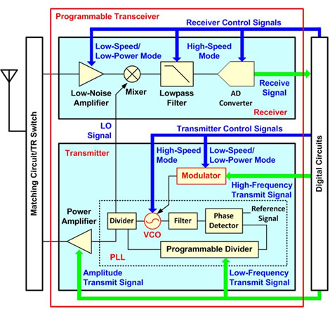
Two points about the new technology are as in Figure 2.
1. Digitally controlled receiver technology
Simplifying the architecture of the transceiver circuit as much as possible has resulted in lower power demands. The digitally controlled transceiver circuit uses a programmable structure that can change its circuitry characteristics to support different phase and frequency modulation methods in adherence to BAN international standards. The receiver consists of a low-noise amplifier, mixer, low-pass filter, and AD converter, and uses a direct-conversion technique that extracts the baseband signal(1) directly from the incoming wireless signal. The use of this technique, along with minimized power requirements for all of the constituent circuitry, made it possible to greatly reduce power requirements. The 4.5-Mbps high-speed mode optimizes the frequency characteristics of the low-pass filter and AD converter through digital circuits. In the 11.7-kbps low-speed, low-power mode, the low-noise amplifier operates at lower power, which degrades its sensitivity, but digital processes compensate for this.
 Figure 2: Transceiver Architecture
2. High-speed digital three-point modulation technology
Using a transmitting mixer in the transmitter makes it easier to implement high-speed mode, but mixers and their driver circuitry are known to greatly increase power demands. A combination of the following three techniques resulted in low-power operation.
- Rather than using a transmitting mixer, the circuitry uses a digital three-point modulation scheme in which a PLL(2), which generates the wireless signal from the digital circuit, takes as input high-frequency and low-frequency signals, and, similarly, the amplified transmit signal is input to the power amplifier.
- To implement the high-speed mode using digital three-point modulation, a dual-varactor circuit technology was developed that, when in high-speed mode, increases the variation in the varactor's(3) capacitance at the VCO(4), which takes the high-frequency modulated signal as input.
- For low-speed/low-power mode, a low-power technology was developed that reduces the VCO modulation circuit's baseline current by 90% while still allowing modulation.
These technologies support both a low-speed mode and high-speed mode with more than 300 times the transfer rate, resulting in a maximum power consumption of 1.6 mW when receiving and 1.8 mW when transmitting.
Results
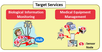
This transceiver circuit for healthcare applications has potential applications beyond patient monitoring, and could be used as a sensing front-end interface for medical-device management (Figure 3). In both applications, the lifespan of the batteries used in the sensor nodes will be greatly extended, relieving the burden on patients and making operations more efficient for medical practitioners.
 Figure 3: Applications of BAN
Future Plans
Based on the newly developed wireless transceiver technology, Fujitsu Laboratories plans to extend its application beyond medicine and healthcare, applying it as a fundamental network front-end technology for use in such areas as agriculture and livestock management, monitoring of societal infrastructure and structures, factory monitoring, and environmental monitoring.
About Fujitsu
Fujitsu is the leading Japanese information and communication technology (ICT) company offering a full range of technology products, solutions and services. Approximately 170,000 Fujitsu people support customers in more than 100 countries. We use our experience and the power of ICT to shape the future of society with our customers. Fujitsu Limited (TSE:6702) reported consolidated revenues of 4.4 trillion yen (US$47 billion) for the fiscal year ended March 31, 2013. For more information, please see http://www.fujitsu.com.
About Fujitsu Laboratories
Founded in 1968 as a wholly owned subsidiary of Fujitsu Limited, Fujitsu Laboratories Limited is one of the premier research centers in the world. With a global network of laboratories in Japan, China, the United States and Europe, the organization conducts a wide range of basic and applied research in the areas of Next-generation Services, Computer Servers, Networks, Electronic Devices and Advanced Materials. For more information, please see: http://jp.fujitsu.com/labs/en.
About imec Holst Centre
Holst Centre is an independent open-innovation R&D centre that develops generic technologies for Wireless Autonomous Transducer Solutions and for Systems-in-Foil. A key feature of Holst Centre is its partnership model with industry and academia around shared roadmaps and programs. It is this kind of cross-fertilization that enables Holst Centre to tune its scientific strategy to industrial needs.
Holst Centre was set up in 2005 by imec (Flanders, Belgium) and TNO (The Netherlands) with support from the Dutch Ministry of Economic Affairs and the Government of Flanders. It is named after Gilles Holst, a Dutch pioneer in Research and Development and first director of Philips Research.
Located on High Tech Campus Eindhoven, Holst Centre benefits from the state-of-the-art on-site facilities. Holst Centre has over 180 employees from around 28 nationalities and a commitment from more than 45 industrial partners.
Visit us at www.holstcentre.com
About imec
Imec performs world-leading research in nanoelectronics. Imec leverages its scientific knowledge with the innovative power of its global partnerships in ICT, healthcare and energy. Imec delivers industry-relevant technology solutions. In a unique high-tech environment, its international top talent is committed to providing the building blocks for a better life in a sustainable society. Imec is headquartered in Leuven, Belgium, and has offices in Belgium, the Netherlands, Taiwan, US, China, India and Japan. Its staff of over 2,080 people includes more than 670 industrial residents and guest researchers. In 2012, imec's revenue (P&L) totaled 320 million euro. Further information on imec can be found at www.imec.be. Stay up to date about what's happening at imec with the monthly imec magazine, available for tablets and smartphones (as an app for iOS and Android), or via the website www.imec.be/imecmagazine
Press Contacts
Public and Investor Relations Division
Inquiries
Company:Fujitsu Limited
Imec is a registered trademark for the activities of IMEC International (a legal entity set up under Belgian law as a "stichting van openbaar nut"), imec Belgium (IMEC vzw supported by the Flemish Government), imec the Netherlands (Stichting IMEC Nederland, part of Holst Centre which is supported by the Dutch Government), imec Taiwan (IMEC Taiwan Co.) and imec China (IMEC Microelectronics (Shanghai) Co. Ltd.) and imec India (Imec India Private Limited).
All other company or product names mentioned herein are trademarks or registered trademarks of their respective owners. Information provided in this press release is accurate at time of publication and is subject to change without advance notice.
Date: 12 February, 2014
City: Kawasaki, Japan, and Eindhoven, The Netherlands
Company:
Fujitsu Laboratories Ltd.,
,
imec Holst Centre,
,
,
,
,
,
,
,
,
,
,
![]() E-mail: mban_press_2014@ml.labs.fujitsu.com
E-mail: mban_press_2014@ml.labs.fujitsu.com