![]()
Archived content
NOTE: this is an archived page and the content is likely to be out of date.
Fujitsu Develops First Optical Transmission Technology to Achieve 100 Gbps Using 10 Gbps Transmission Components
Paves the way for 400 Gbps Ethernet transceivers in next-generation datacenters
Fujitsu Laboratories Ltd.,Fujitsu Research and Development Center Co., Ltd.
Fujitsu Laboratories Limited and Fujitsu Research and Development Center Co., Ltd. of China today announced the development of the world's first optical-transmission technology that can achieve 100 Gbps transmission speeds using widely available, conventional components intended for 10 Gbps networking.
Increasing data-transfer rates has typically required new components designed for those higher speeds, for which existing components have not been compatible. Moreover, there is a limit to the speed improvements that can be achieved with transmission methods using the simple modulation and demodulation formats that have been used to date. Fujitsu Laboratories and Fujitsu R&D Center have applied a Discrete Multi-Tone (DMT) modulation/demodulation format(1) using digital signal processing (DSP) to transmit at 100 Gbps per channel using conventional components intended for transmission speeds of 10 Gbps per channel.
Applying this technology to an optical transceiver with four channels would result in a 400 Gbps Ethernet transceiver, which are needed in the next generation of datacenters in order to increase their data transmission speeds and processing capacity to better support cloud services.
Details of this technology are being presented at the Optical Fiber Communication Conference and National Fiber Optic Engineers Conference (OFC/NFOEC 2013), beginning March 17 in Anaheim, California. They will be demonstrated at the Fujitsu Optical Components Limited booth as "DMT Modulation Format 400GbE Transmission Demonstration".
Background
The recent spread of cloud computing and cloud services has heightened the need for better data-processing capabilities and faster data-transfer speeds in datacenters. The optical transceivers in use today have four channels carrying a total of 100 Gbps. For the next generation of datacenters, there is a demand for Ethernet transceivers that are able to deliver 400 Gbps.
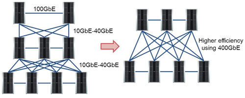 Figure 1: Scope of application for this technology
Technological Issues
Increasing data transfer speeds requires faster transmitting and receiving circuits. However, with previous technology, existing parts could not be used, requiring new electronic and optical components compatible with the higher speeds. In addition, the simple modulation/demodulation method, in which the on/off states of the optical signal correspond to the 1/0 states of the digital signal, has limited the increase in speed.
About the New Technology
Through the application of digital signal processing, which uses the DMT modulation/demodulation format, Fujitsu Laboratories and Fujitsu R&D Center were able to use standard direct-modulation laser components designed for 10 Gbps transmissions to achieve transmission speeds of 100 Gbps per channel. Key features of the new technology are as follows.
1. DMT modulation/demodulation format
While the DMT modulation/demodulation format is used in xDSL(2), this is the first time it has been used for optical transmissions at 100 Gbps. DMT divides the data into multiple subcarriers (carrier waves), and multi-level modulation is used for each subcarrier to achieve high transmission speeds (Figure 2). To optimize each subcarrier's power and number of multiple values, an algorithm was developed that checks receiving conditions between optical transceivers at the time the system is started up and optimizes power and the number of multiple values to suit the transceivers and line conditions.
2. Uses widely available, conventional components
Fujitsu Laboratories and Fujitsu R&D Center have developed a technology that uses existing commodity parts to achieve DMT modulation/demodulation. For example, some components have the characteristic of not being able to maintain sufficient linearity. These components can be profiled in advance and compensated for, enabling them to be used in the same way as parts that do maintain linearity.
Applying this technology to an optical transceiver with four channels (Figure 3) would result in 400 Gbps Ethernet transceivers, which are needed in the next generation of datacenters.
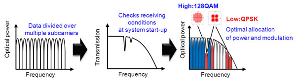 Figure 2: DMT modulation technology
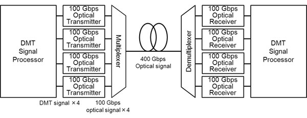 Figure 3: Diagram of the envisioned 4-channel optical transceiver configuration
Results
Through the use of this technology, high-speed transmissions at 100 Gbps were achieved using conventional components, opening the way to higher data transmission speeds and processing capacity at datacenters that support cloud services.
Future Plans
With an eye toward practical use of this technology, an integrated DMT modem is under consideration, and additional improvements for using existing technologies are proceeding.
-
[1] Discrete multitone modulation/demodulation format
A format that divides data among multiple subcarriers (carrier waves), and multi-level modulation is used for each subcarrier to achieve high transmission speeds.
-
[2] xDSL
A high-speed digital data communications technology using phone lines.
About Fujitsu
Fujitsu is the leading Japanese information and communication technology (ICT) company offering a full range of technology products, solutions and services. Over 170,000 Fujitsu people support customers in more than 100 countries. We use our experience and the power of ICT to shape the future of society with our customers. Fujitsu Limited (TSE:6702) reported consolidated revenues of 4.5 trillion yen (US$54 billion) for the fiscal year ended March 31, 2012. For more information, please see http://www.fujitsu.com.
About Fujitsu Laboratories
Founded in 1968 as a wholly owned subsidiary of Fujitsu Limited, Fujitsu Laboratories Limited is one of the premier research centers in the world. With a global network of laboratories in Japan, China, the United States and Europe, the organization conducts a wide range of basic and applied research in the areas of Next-generation Services, Computer Servers, Networks, Electronic Devices and Advanced Materials. For more information, please see: http://jp.fujitsu.com/labs/en.
About Fujitsu Research and Development Center
Established in 1998, Fujitsu Research and Development Center Co., Ltd. is a wholly owned R&D center of Fujitsu Limited, located in Beijing. The center's research areas cover the major business fields of the Fujitsu Group, including information processing, telecommunications, semiconductors, and software and services.For more information, please visit: http://cn.fujitsu.com/frdc/.
Technical Contacts
Network Systems LaboratoriesPhotonics Lab.
![]() E-mail: fjl_dmt@ml.labs.fujitsu.com
E-mail: fjl_dmt@ml.labs.fujitsu.com
Company:Fujitsu Laboratories Ltd.
All company or product names mentioned herein are trademarks or registered trademarks of their respective owners. Information provided in this press release is accurate at time of publication and is subject to change without advance notice.
This press release has been revised as of December 17, 2018.
Date: 14 March, 2013
City: Kawasaki, Japan, and Beijing, China
Company:
Fujitsu Laboratories Ltd.,
Fujitsu Research and Development Center Co., Ltd.,
,
,
,
,
,
,
,
,