![]()
Archived content
NOTE: this is an archived page and the content is likely to be out of date.
Fujitsu Develops World's First Process Technology for Copper-Internal-Electrode-based Capacitors for High-Speed LSIs
Improves current-flow efficiency by 10-fold; contributes toward development of next-generation high-speed computers
Fujitsu Laboratories Ltd.
Fujitsu Laboratories Ltd. today announced the development of a process technology to produce capacitors(1) for high-speed LSI chips, which as a world's first employs copper for internal electrodes. The use of copper for internal electrodes lowers the impedance(2) of the capacitor itself, and by mounting the capacitor directly below the LSI chip, impedance from the circuits can also be reduced, resulting in increase of current-flow efficiency by 10 times compared to previously available technology. The new technology is expected to enable the next generation of high-speed computers to operate at even higher speeds.
Background
As LSI chips continue to achieve higher speeds and higher integration densities, and with many of a chip's elements all operating simultaneously, much of the current used by the chip is consumed in bursts. This can lower voltages, which may impact proper operation. In those instances in which much current is consumed, it is desirable to mount a capacitor near the LSI chip to instantly supplement the current.
Technological Challenges
Conventionally, ceramic-chip condensers being used as power-supply capacitors have been mounted on the surface or rear of the circuit board or LSI chip package, supplying current to the LSI chip through the circuit wires (Figure 1). This method results in a relatively long electrical pathway between the capacitor and LSI chip, which raises impedance and would potentially create instabilities in future high-speed computers. In addition, because nickel, which has comparatively high resistance, has conventionally been used for the internal electrodes in the capacitor, the impedance of the capacitor itself has been high, limiting the speed of the power-supply current.
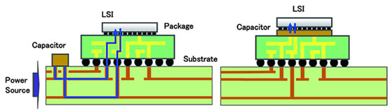 Figure 1: Mounted structure of conventional power-supply capacitor (left) and Fujitsu's new power-supply capacitor (right)
Larger View (37 KB)
Newly-developed Technology
Fujitsu Laboratories developed a basic manufacturing method for capacitors that can provide high-speed, stable supply of current to an LSI chip (Figure 2).
The production of capacitors with the following key characteristics has been made possible using nano-particle deposition technology(3):
- Internal electrodes made using low-resistance copper (a world's first)
- Ultra-fine through-hole contact construction enabling connection directly beneath the LSI chip
- High-reliability thin-film dielectric layer enabling high capacitance (1 µF/cm2·layer)
 Figure 2: Manufacturing process for Fujitsu's newly-developed capacitor
Larger View (183 KB)
Results
Employing copper for the internal electrodes to lower the impedance of the capacitor itself reduces the length of the circuits between the capacitor and the LSI chip, making it is possible to limit impedance of the power-supply line. These factors together result in a power supply that is 10 times as efficient for operationally stable high-speed LSI chips, a development that is expected to contribute to higher computer speeds.
Future Developments
Fujitsu Laboratories will continue with development of technologies to enable miniaturization of the capacitor terminals and multi-layering, aiming to apply this new technology to computers around 2015.
-
[1] Capacitor
An element that accumulates electrical charge. Used to suppress variations in power-supply voltages that result from high-speed operations.
-
[2] Impedance
Resistance in alternating currents (relative to voltage and current).
-
[3] Nano-particle deposition technology
A method for forming inorganic films using nano-scale ceramic particles.
About Fujitsu Laboratories
Founded in 1968 as a wholly owned subsidiary of Fujitsu Limited, Fujitsu Laboratories Limited is one of the premier research centers in the world. With a global network of laboratories in Japan, China, the United States and Europe, the organization conducts a wide range of basic and applied research in the areas of Next-generation Services, Computer Servers, Networks, Electronic Devices and Advanced Materials. For more information, please see: http://jp.fujitsu.com/labs/en.
Technical Contacts
Environment & Energy Research Center
![]() Phone: +81(46)250-8389
Phone: +81(46)250-8389
![]() E-mail: asd-press@ml.labs.fujitsu.com
E-mail: asd-press@ml.labs.fujitsu.com
Company:Fujitsu Laboratories Ltd.
Company and product names mentioned herein are trademarks or registered trademarks of their respective owners. Information in this press release is accurate at time of publication and is subject to change without advance notice.
Date: 02 February, 2011
City: Kawasaki, Japan
Company:
Fujitsu Laboratories Ltd.,
,
,
,
,
,
,
,
,
,