![]()
Archived content
NOTE: this is an archived page and the content is likely to be out of date.
Fujitsu Develops Technology to Manufacture Power-Supply Transistors On Nearly Any Flat-surface Material
Paves the way to manufacturing power-supply circuits on copper, glass, or plastic; not limited to circuit boards
Fujitsu Laboratories Ltd.
Fujitsu Laboratories Ltd. today announced the development of a technology that enables the manufacture of power-supply transistors on nearly any flat surface, including glass, plastic, or copper. High breakdown-voltage was achieved by forming a high breakdown-voltage power-supply transistor on a target substance using zinc-oxide (ZnO) material and protecting the transistor's channel using a polymer layer. This new technology will enable power-supply circuits to be manufactured on a wide range of flat surfaces, with potential applications including sensors and piezoelectric devices.
Details of this technology were presented at the 2010 Materials Research Society Fall Meeting (2010 MRS Fall Meeting), being held in Boston from November 29 - December 3.

Larger View (48 KB) |

Larger View (36 KB) |
Background
A major issue in reducing environmental footprints is reducing the power consumed by electrical power supplies in applications such as IT equipment, household appliances, and automobiles. At the same time, demand to lower the costs of general-purpose power-supply circuits has generated anticipation for the realization of low-cost power-supply transistors which feature high breakdown-voltages.
Zinc oxide is a wide band-gap(1) semiconductor material that can be used as a power-supply transistor with low loss, and is a material that has potential for creating transistors on nearly any flat surface (Figure 1). Recently, there has been R&D underway for forming zinc oxide on glass substrates for transistors for liquid-crystal-display (LCD) televisions and monitors.
Technological Challenges
Fabricating ZnO as a power-supply transistor with high breakdown-voltage presents the challenge of lowering the density of the channel material - which is required for high breakdown-voltage - while suppressing the charge trap resident in the surface of the material, which can cause electrical-field concentration. These issues needed to be resolved in order to develop a technology that would allow for ZnO to be used as a high breakdown-voltage transistor in power supplies.
Newly-Developed Technology
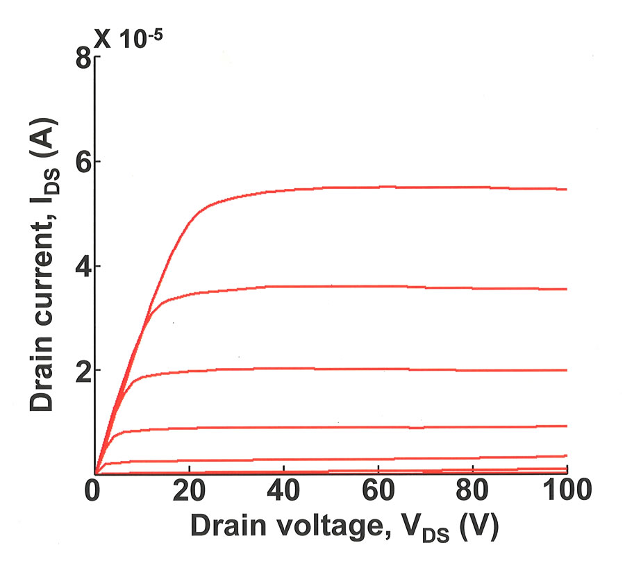
By employing indium-gallium-zinc-oxide (IGZO) as the material and protecting the transistor's channel with a polymer layer (Figure 2), Fujitsu Laboratories was able to produce a 100-V transistor for use in power supplies (Figure 3). In addition, because the high breakdown-voltage transistor can be manufactured directly on copper substrate which is used as a packaging material, heat dissipation is simplified and more easily achieved, and costs can be reduced.
 Figure 2: Cross section showing protective film
Larger View (41 KB)
 Figure 3: Characteristics of a transistor with protective film
Larger View (55 KB)
Results
The new technology can be applied to power circuits formed on any flat-surface material, and can be used for such applications as high-voltage sensors and piezoelectronic devices.
Future Plans
Fujitsu Laboratories will continue refine this new technology to make it suitable for power-supply transistors by further increasing the breakdown voltage and lowering the on-state resistance, and will strive toward incorporation of this technology in IT products around 2015.
For more information:
-
[1] Wide band-gap transistor
A transistor that has a wide band-gap. Typically, the breakdown voltage of a transistor will rise in proportion to its band-gap.
About Fujitsu Laboratories
Founded in 1968 as a wholly owned subsidiary of Fujitsu Limited, Fujitsu Laboratories Limited is one of the premier research centers in the world. With a global network of laboratories in Japan, China, the United States and Europe, the organization conducts a wide range of basic and applied research in the areas of Next-generation Services, Computer Servers, Networks, Electronic Devices and Advanced Materials. For more information, please see: http://jp.fujitsu.com/labs/en.
Technical Contacts
Energy Technology LaboratoryEnvironment & Energy Research Center
![]() Phone: +81(46)250-8234
Phone: +81(46)250-8234
![]() E-mail: nano-mate@labs.fujitsu.com
E-mail: nano-mate@labs.fujitsu.com
Company:Fujitsu Laboratories Ltd.
Company and organization names mentioned herein are trademarks or registered trademarks of their respective owners. Information provided in this press release is accurate at time of publication and is subject to change without advance notice.
Date: 03 December, 2010
City: Kawasaki, Japan
Company:
Fujitsu Laboratories Ltd.,
,
,
,
,
,
,
,
,
,