![]()
Archived content
NOTE: this is an archived page and the content is likely to be out of date.
Fujitsu and University of Tokyo Achieve World's First 25Gbps Data Communication Using Quantum Dot Laser
Enables use of quantum dot lasers as an optical source for future high-speed data communications
Fujitsu Limited,Fujitsu Laboratories Ltd.,University of Tokyo
Fujitsu Limited, Fujitsu Laboratories Ltd., and the University of Tokyo today announced the world's first quantum dot laser(1) -based 25 Gbps high-speed data transmission. Quantum dot lasers are a type of laser being anticipated as a next-generation semiconductor laser capable of handling high-speed data transmissions while consuming minimal power. As increasing the number of quantum dots is known to improve a quantum dot laser's operation speed, layers of quantum dots with a higher density than conventionally employed were stacked, thereby doubling the laser's operation speed and enabling a significant improvement over previous technologies. This new technology is expected to be employed for optical sources for next-generation high-speed data communications(2) that aim to achieve data transmission speeds of 100 Gbps, ten times faster than current data transmission speeds.
Details of the technology will be presented at the Conference on Lasers and Electro-Optics and the Quantum Electronics and Laser Science Conference (CLEO/QELS 2010), being held from May 16 - 21 in San Jose, U.S. Part of this research belongs to a project contracted to the Photonics Electronics Technology Research Association (PETRA) by the New Energy and Industrial Technology Development Organization (NEDO), while part of the research was carried out under Japan's Ministry of Education, Culture, Sports, Science and Technology's Special Coordination Funds for Promoting Science and Technology. In addition, joint research and development of quantum dot lasers is being pursued through collaboration between Professor Yasuhiko Arakawa's laboratory at the University of Tokyo, Fujitsu, Fujitsu Laboratories, and QD Laser, Inc.
About Quantum Dot Lasers
Quantum dot lasers are semiconductor lasers which employ quantum dots - nanometer-sized semiconductor particles as an active material for lasing, which Fujitsu and Fujitsu Laboratories have developed in an industrial-academic collaboration with Professor Yasuhiko Arakawa's laboratory of the University of Tokyo. Quantum dot lasers feature significant advantages over other types of semiconductor lasers, such as being less sensitive to temperature fluctuations, while offering tremendous advances over previous semiconductor lasers in terms of lower power consumption, greater transmission distances, and faster speeds. Thus, there is much anticipation for quantum dot lasers to become a core technology for developing high-performance optical sources in the future, when there will be a tremendous rise in data traffic of optical communications.
Background
In accordance with the growth of broadband Internet bandwidths attributable to emerging services, such as cloud computing services and high-definition video download services, there has been rapid increase in such network traffic. In order to keep pace with data transmission volumes that continue to grow larger each year, optical networks need to run faster and be expanded to handle higher volumes of data.
Currently, 10 Gbps transmissions are the mainstream for data transmission. However, in view of the fact that transmission speeds are continually becoming faster, currently 100 Gbps Ethernet ("100 GbE") - which features data transmission speeds ten times as fast as currently available - is being promoted as an international standard(3) for next-generation high-speed data communications. Accordingly, there is a need for laser light sources that can handle such next-generation high-speed data transmissions, while consuming only low power.
Technological Challenges
Quantum well lasers(4), which have conventionally been used as optical sources for data communications, have a problem of dramatic increases in power consumption attributable to increased driving current when temperatures rise. The quantum dot laser developed by Fujitsu Laboratories and the University of Tokyo uses 3-dimensional (3D) semiconductor nanostructures to produce quantum effects, thus giving it excellent characteristics, including stable operation over a range of temperatures and low power consumption. However, the quantum dot laser had been limited to handling data transfer speeds up to 10 Gbps.
Overview of Newly-developed Technology
In order to increase the speed of quantum dot lasers, it was necessary to increase the laser's optical gain, which in turn required an increase in the number of underlying quantum dots. New quantum dot fabrication technology was developed and applied, resulting in a quantum dot laser capable of high-speed operations at 25 Gbps.
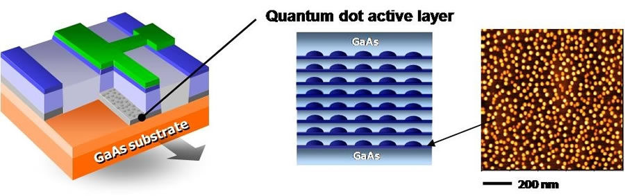
Key features of the newly-developed technologies are as follows (Figure 1):
1. A technology for forming high-density indium-arsenide (InAs) quantum dots on the surface of a gallium-arsenide (GaAs) substrate. This doubles the number of quantum dots per unit area to 6 x 10¹⁰ per 1cm2.
2. A technology for stacking multiple layers of high-density quantum dots. This increases the number of possible layers to 8 layers, an increase from the previously-available 5 layers.
Quantum dots are fabricated using molecular beams in a high-vacuum chamber to embed indium (In) and arsenide (As) in GaAs . Because the atomic distance in InAs is greater than in GaAs, strain is induced in the InAs crystallized on the GaAs substrate. The strain energy can be relaxed by forming 3D crystals, in which each 3D nanocrystal functions as a single quantum dot.
By optimizing the growth conditions in which the 3D crystals are formed, a technology has been developed to double the in-plane area density of the quantum dots to 6 x 10¹⁰ per 1cm2. Technology was also developed that allows 8 layers - instead of 5 layers - to be stacked while preserving the same high-density in-plane.
Fabrication of quantum dots by employing these aforementioned technologies enabled an increase in number of quantum dots, thereby increasing the optical gain. As a world first, a quantum dot laser employing this active layer was successfully tested at 25 Gbps high-speed modulation.
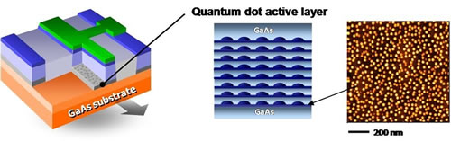 Figure 1: Quantum dot laser featuring an active layer containing high-density arrays of quantum dots
Larger View (60 KB)
Results
This new technology has made it possible to employ temperature-stable, low-power consuming quantum dot laser light sources in a range of next-generation high-speed communications applications, such as 100GbE. Furthermore, it also obviates the need for expensive packages with embedded temperature controllers, thereby helping to lower costs.
Future Developments
This new technology represents a significant step towards the implementation of quantum dot lasers as an optical source for next-generation high-speed communications. Fujitsu Laboratories and the University of Tokyo plan to further refine this technology to increase its transmission distance and to confirm reliability. QD Laser, Inc. is also considering commercializing this technology.
-
[1] Quantum dot lasers
A semiconductor laser in which a quantum dot, which is a 3-dimensional nanostructure, is used as an active material for lasing. Its quantum effects allow it to operate without being dependent on temperature, thus making it possible to significantly reduce fluctuations in optical output that are attributable to temperature changes.
-
[2] Optical sources for next-generation high-speed communications
In order to achieve a transmission speed of 100 Gbps, for distances of 10km to 40km, an international standard is being promoted for a transmission method using a fiber to carry four optical signals, each operating at 25 Gbps and multiplexed together.
-
[3] International standard
100 Gigbit Ethernet (100GbE) is being promoted by the Institutue of Electrical and Electronic Engineers (IEEE) as a standard for Ethernet that can transmit at speeds of 100 Gbps.
-
[4] Quantum well lasers
A type of semiconductor laser in which thin layers - about several nanometers thick - sandwiched between wide bandgap layers are employed as active layers. These thin layers are referred to as quantum well layers. In such structures, confinement of electrons in the quantum well layers improves laser performance, and they are widely used as light source in many applications. However, quantum well lasers used in optical fiber communications are highly sensitive to temperature.
About Fujitsu
Fujitsu is a leading provider of ICT-based business solutions for the global marketplace. With approximately 170,000 employees supporting customers in 70 countries, Fujitsu combines a worldwide corps of systems and services experts with highly reliable computing and communications products and advanced microelectronics to deliver added value to customers. Headquartered in Tokyo, Fujitsu Limited (TSE:6702) reported consolidated revenues of 4.6 trillion yen (US$50 billion) for the fiscal year ended March 31, 2010. For more information, please see: www.fujitsu.com.
About Fujitsu Laboratories
Founded in 1968 as a wholly owned subsidiary of Fujitsu Limited, Fujitsu Laboratories Limited is one of the premier research centers in the world. With a global network of laboratories in Japan, China, the United States and Europe, the organization conducts a wide range of basic and applied research in the areas of Next-generation Services, Computer Servers, Networks, Electronic Devices and Advanced Materials. For more information, please see: http://jp.fujitsu.com/labs/en.
About University of Tokyo
The University of Tokyo was established in 1877 as the first national university in Japan. As a leading research university, the University of Tokyo offers courses in essentially all academic disciplines at both undergraduate and graduate levels and conducts research across the full spectrum of academic activity. The university aims to provide its students with a rich and varied academic environment that ensures opportunities for both intellectual development and the acquisition of professional knowledge and skills.
The University of Tokyo is known for the excellence of its faculty and students and ever since its foundation many of its graduates have gone on to become leaders in government, business, and the academic world. For more information, please see: http://www.u-tokyo.ac.jp/index_e.html.
Technical Contacts
Nanoelectronics Research Center
![]() E-mail: nanoele-photonic@ml.labs.fujitsu.com
E-mail: nanoele-photonic@ml.labs.fujitsu.com
Company:Fujitsu Laboratories Ltd.
Company, organization, and product names mentioned herein are trademarks or registered trademarks of their respective owners. Information provided in this press release is accurate at time of publication and is subject to change without advance notice.
Date: 20 May, 2010
City: Tokyo and Kawasaki, Japan
Company:
Fujitsu Limited,
Fujitsu Laboratories Ltd.,
University of Tokyo,
,
,