![]()
Archived content
NOTE: this is an archived page and the content is likely to be out of date.
Fujitsu Laboratories Develops World's First CMOS-based Power Amplifier Operating at 77GHz
-Realizes millimeter-waveband power amplifiers using 90nm CMOS process technology-
Fujitsu Laboratories Ltd.
Fujitsu Laboratories, Ltd. today announced the development of a millimeter-waveband power amplifier (PA) using standard 90nm CMOS process technology. Targeting millimeter-wave applications, Fujitsu Labs developed a standard CMOS modeling technology and design techniques to minimize high-frequency signal loss, thereby enabling the development of the world's first CMOS-based PA that operates at 77GHz. The technology realizes CMOS radio frequency (CMOS RF) front-end circuitry that includes a PA, thereby enabling integration with baseband circuitry(1) on a single chip, for use in millimeter-wave automotive radar systems.
This technology will be presented at the International Solid-State Circuits Conference (ISSCC) 2008 to be held in San Francisco from February 3-7. (Session 31.3).
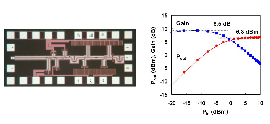
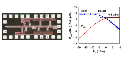 Figure 1: Chip and Input-Output characteristics for Fujitsu Labs' 77GHz PA
Larger View (146 KB)
Background
The millimeter wave is ideal for measuring with high resolution and accuracy the distance between two points, as well as for high-capacity data transmission. As such, the millimeter wave is starting to be applied to automotive radar systems and to wireless transmission systems. Typically, compound semiconductors have been used in the RF front-end circuits(2) of these systems in order to realize high gain and output of high-frequency signals. On the other hand, for CMOS technology, which features high levels of integration and high-functionality, progress has been made in regard to operational speeds - attributable to ongoing miniaturization - and it is now possible to apply millimeter wave circuits to achieve operation that was previously achieved through compound semiconductors.
Technological Challenges
Practical application of standard CMOS technology in millimeter-wave circuitry has been problematic due to the occurrence of significant signal loss. In order to boost the gain in an amplifier, a number of factors that are not evident on a circuit diagram, such as parasitic capacitance(3), need to be accurately reflected. In addition, signal loss in a matching circuit(4) needs to be suppressed to enable maximum amplification performance.
Fujitsu Labs' New Technology
Fujitsu Labs developed the following two technologies that make it possible to apply standard CMOS technology to millimeter-wave amplifiers.
1. Modeling technology for transistors and passive components operating in the millimeter waveband
Fujitsu Labs established a transistor model that shows the operating characteristics at millimeter-waveband and developed parameter-extraction method technology. Researchers also optimized the structure of transmission lines, capacitors, and other passive components, and developed structures that minimize resistive losses.
2. Matching circuit design
To keep the circuitry compact, Fujitsu Labs developed a "short stub"(5) matching circuit and integrated it with the power-supply circuitry in a way that would further reduce signal losses. This reduced the amount of chip space required by the matching circuit to one-tenth previous levels, and also reduced signal loss to 0.4 decibels (0.4 dB).
Results
The combination of these two technologies resulted in the world's first PA operating at 77GHz to achieve 8.5 dB gain and 6.3 decibel milliwatts (6.3dBm) saturated output power (see Figure 1). Furthermore, a separate PA operating at 60GHz was developed and achieved 8.3 dB of gain and 10.6 dBm saturated output power.
Fujitsu Labs' new technology makes it possible to implement 77GHz automotive radars using inexpensive standard CMOS technologies. These developments could also be used to extend the transmission range of wireless communications systems in the 60GHz band.
Furthermore, by combining baseband circuitry with RF front-end circuitry on one chip, millimeter-waveband transceiver chips - which had been expensive to produce in the past - can now be made considerably smaller. As a result, widespread application of millimeter-waveband technologies in both automotive radar systems and wireless communications systems is anticipated in the future.
Future Developments
Fujitsu Labs plans to utilize standard CMOS technologies to further develop amplifier circuits with higher output power, and integrated RF front-end circuits. Leveraging these technologies, Fujitsu Labs will conduct research to develop chips for millimeter-wave automotive radar systems and wireless communications systems.
For more information:
-
[1] Baseband circuitry
In wireless communications circuitry, the circuitry that processes the data signal before it is modulated to a high frequency.
-
[2] RF front-end circuits
In wireless communications circuitry, the circuit that pre-processes the high-frequency signal.
-
[3] Parasitic capacitance
Static capacitance that exists between a transistor's I/O electrode and other peripheral electrodes. The amount varies depending on the distance between components and their sizes, making it difficult to actualize in normal circuit design.
-
[4] Matching circuit
In RF circuit design, a circuit that produces conditions allowing for maximum power input to following stage.
-
[5] Short stub
In a transmission line of arbitrary length, this refers to a transmission line in which one end is connected to the inside of a circuit, and the other end is connected to a power source or ground so that the electrical potential of a RF signal is always zero.
About Fujitsu Laboratories
Founded in 1968 as a wholly owned subsidiary of Fujitsu Limited, Fujitsu Laboratories Limited is one of the premier research centers in the world. With a global network of laboratories in Japan, China, the United States and Europe, the organization conducts a wide range of basic and applied research in the areas of Multimedia, Personal Systems, Networks, Peripherals, Advanced Materials and Electronic Devices. For more information, please see:http://jp.fujitsu.com/group/labs/en/
Technical Contacts
Advanced Devices Lab.Device & Materials Laboratories
![]() Phone: +81-46-250-8244
Phone: +81-46-250-8244
![]() E-mail: amr@ml.labs.fujitsu.com
E-mail: amr@ml.labs.fujitsu.com
Company:Fujitsu Laboratories Ltd.
All company or product names mentioned herein are trademarks or registered trademarks of their respective owners. Information provided in this press release is accurate at time of publication and is subject to change without advance notice.
This press release has been revised as of December 17, 2018.
Date: 04 February, 2008
City: Kawasaki
Company:
Fujitsu Laboratories Ltd.,
,
,
,
,