![]()
Archived content
NOTE: this is an archived page and the content is likely to be out of date.
Fujitsu Develops Highly-Reliable Multi-Layer Interconnect Technology for Logic LSI Devices for 32nm Generation and Beyond
- Enables both lowering of line resistance in interconnects and high reliability, vital for 32nm generation technology -
Fujitsu Laboratories Ltd.,Fujitsu Limited
Fujitsu Laboratories Ltd. and Fujitsu Limited today announced their development of technology that enables high-reliability multi-layer interconnects for logic LSIs for 32nm generation and beyond, by using copper with manganese additives in combination with an ultra-thin film barrier metal. Compared to conventional technology, Fujitsu's new technology effectively reduces line resistance in interconnects, and increases endurance against electro-migration(1) - a cause of LSI degradation over time. This technology will enable Fujitsu to provide highly-integrated high-performance LSIs to customers.
Details of this technology were presented at the IEDM (International Electron Devices Meeting), held from December 10 - 12 in Washington, D.C. (Session: 19.6).
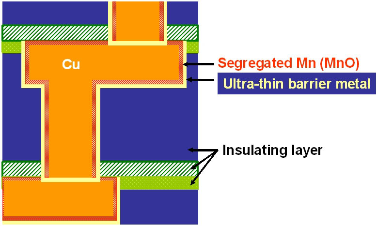
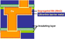 Figure 1: Fujitsu's newly-developed multi-layer interconnect structure
Larger View (70 KB)
Background
In accordance with electronic devices becoming further compact, as microprocessors becoming increasingly higher in performance and mobile information devices become more multi-functional, there is a growing demand for high-performance, logic LSI devices that feature higher levels of integration and consume less power, a trend that is also driving the development of finer interconnects used in LSI devices. For example, the 32nm generation of logic LSIs that are currently under development will be using copper interconnects measuring 50nm wide. In order to enable the development of higher-performance LSIs, technology capable of achieving high reliability becomes necessary, by limiting the rise of interconnect resistance while in addition reducing age degradation of interconnects.
Technological Challenges
Up through the 45nm generation of LSIs, copper interconnects were wrapped in a barrier metal for protection. The barrier metal is necessary to prevent the diffusion of copper into the insulating film, and to prevent the insulating film from oxidizing the copper. A thick barrier metal improves reliability, but at the 32nm generation level of miniaturization, the barrier metal would occupy a disproportionate amount of space relative to the copper interconnect, thereby increasing the line resistance of the interconnect. Thus, the need to reduce line resistance while maintaining reliability has become a pressing issue.
Key Features of the New Technology
By forming copper with manganese additives on an ultra-thin film barrier metal, Fujitsu succeeded in reducing interconnect line resistance, while maintaining high reliability. This interconnect structure (see Figure 1) is formed through the following processes:
- An ultra-thin film barrier metal is formed on the insulating layer to prevent copper diffusion.
- A seed layer of copper containing manganese is formed and then plated with the copper interconnect material.
- In a following process, the structure is heated to a temperature above 350 degrees Celsius, which creates a manganese segregation layer - thinner than the barrier metal – that enwraps the copper interconnects.
The use of a manganese segregation layer has made it possible to maintain existing barrier performance, as it prevents oxidation of the ultra-thin film barrier metal.
Results
Compared to the copper interconnect barrier metal combination method that had been used up to the 45nm generation, this new technique from Fujitsu for multi-layer interconnects enables the reduction of thickness of barrier-metal films by one-third, and effectively reduces interconnect line resistance to levels that meet the standards laid out for the 32nm generation in the International Technology Roadmap for Semiconductors (ITRS)(2). In addition, by increasing endurance lifetime against electro-migration – a cause for degradation over time - by a factor of 47, high reliability applicable for highly integrated minute interconnects for the 32nm generation and beyond is achieved.
Future Developments
This new technology paves the way for multi-layer interconnect technology applicable for logic LSIs for the 32nm generation and beyond. Fujitsu plans to further develop this technology to provide high-performance highly integrated power efficient LSIs.
-
[1] Electro-migration
A phenomenon that occurs when high-density current flows, in which copper atoms in a wire gradually move and create voids which grow, thereby increasing interconnect line resistance. In extreme cases, this can result in the wire being severed. As this phenomenon will become more prominent as densities of currents will increase for 32nm generation technology and beyond, developing a countermeasure is of major importance.
-
[2] International Technology Roadmap for Semiconductors (ITRS)
A roadmap for semiconductor development, created annually by representatives from Japan, the US, Europe, South Korea, and Taiwan. For more information: http://www.itrs.net/
About Fujitsu Laboratories
Founded in 1968 as a wholly owned subsidiary of Fujitsu Limited, Fujitsu Laboratories Limited is one of the premier research centers in the world. With a global network of laboratories in Japan, China, the United States and Europe, the organization conducts a wide range of basic and applied research in the areas of Multimedia, Personal Systems, Networks, Peripherals, Advanced Materials and Electronic Devices. For more information, please see:http://jp.fujitsu.com/group/labs/en/
About Fujitsu
Fujitsu is a leading provider of customer-focused IT and communications solutions for the global marketplace. Pace-setting device technologies, highly reliable computing and communications products, and a worldwide corps of systems and services experts uniquely position Fujitsu to deliver comprehensive solutions that create infinite possibilities for its customers' success. Headquartered in Tokyo, Fujitsu Limited (TSE:6702) reported consolidated revenues of 5.1 trillion yen (US$43.2 billion) for the fiscal year ended March 31, 2007. For more information, please see: www.fujitsu.com
Technical Contacts
Silicon Technologies Development Lab
![]() Phone: +42-532-1253
Phone: +42-532-1253
![]() E-mail: silicon-ask@ml.labs.fujitsu.com
E-mail: silicon-ask@ml.labs.fujitsu.com
Company:Fujitsu Laboratories Limited
All company or product names mentioned herein are trademarks or registered trademarks of their respective owners. Information provided in this press release is accurate at time of publication and is subject to change without advance notice.All product names and company names mentioned herein are the trademarks or registered trademarks of their respective firms.
Date: 12 December, 2007
City: Tokyo
Company:
Fujitsu Laboratories Ltd.,
Fujitsu Limited,
,
,
,