Archived content
NOTE: this is an archived page and the content is likely to be out of date.
Fujitsu Develops GaN HEMT Technology for Next-generation Mobile Phone Base Station Amplifiers
Fujitsu Laboratories Ltd.
Kawasaki, December 05, 2005
Fujitsu Laboratories Limited today announced the development of the world's first gallium nitride(1) (GaN) high electron-mobility transistor (HEMT)(2) with insulated gates(3) capable of practical output levels of 100 watts (W) or higher. By reducing gate leakage current to less than one-one millionth that of conventional levels, the technology paves the way for high-efficiency operation of high power GaN HEMTs for amplifiers of next-generation mobile phone base stations.
Fujitsu's new technology will play an important role in reducing power consumption of transmission amplifiers used in next- and future-generation mobile phone base station systems.
Details of this technology will be presented at the IEEE International Electron Devices Meeting (IEDM) to be held in Washington, D.C. from December 5.
Background
As transmission speeds are becoming faster for wireless communications, the power consumption of mobile phone base stations will increase. In order to realize base stations with lower power consumption, GaN HEMT amplifiers are currently being developed. Next- and future-generation networks will have greater output levels, necessitating much higher power efficiency to dramatically reduce the increased power consumption. However, applying existing GaN HEMT technology to reduce power consumption had proven problematic due to the fact that gate leakage current increases as power efficiency rises, creating problems in terms of reliability and amplification characteristics.
Technological Challenges
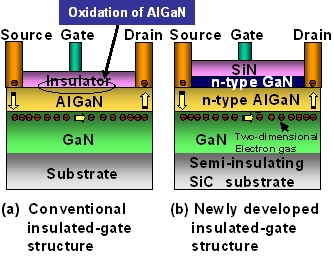
To improve the gate leakage current, there is a method which employs the insertion of an insulation layer directly below the gate. However, this results in the formation of a very large area in which electron movement is impaired, known as the "interface trap(4)" region, resulting from the surface contact between the insulation layer and semiconductor. This in turn impaired the amplification of the electrical signal applied at the gate electrode and degraded the transistor's output characteristics. As a result, no output beyond 100W could be obtained thus far. This is attributable to the fact that the semiconductor surface in contact with the insulation layer used a layer of aluminum gallium nitride (AlGaN), which contains aluminum. Aluminum oxidizes easily, which leads to degradation of performance.
Newly Developed Technology
Fujitsu succeeded in overcoming the technological obstacles by modifying the surface structure of GaN HEMT. This transistor (patent pending) consists of insulated film of silicon nitride deposited on the outermost layer of a GaN HEMT crystal, that has a thin film of n-type doped GaN. By using a GaN layer for the semiconductor surface, instead of an AlGaN layer, which was conventionally used with insulated gate transistors, Fujitsu succeeded in preventing oxidation of the aluminum surface.
Results
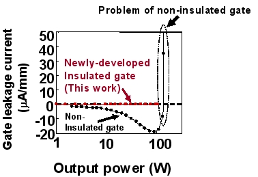
Fujitsu succeeded in reducing gate leakage current to 0.1 microampere or less, which is less than one-one millionth that of conventional technologies that do not use insulated gates.
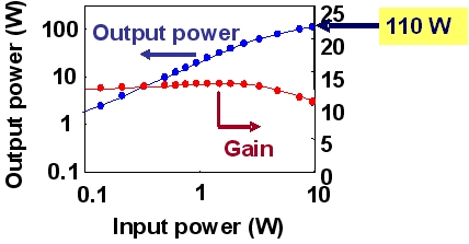
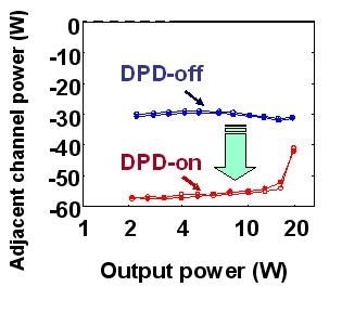
Performance was also improved, with maximum output of 110 W achieved. This is the world's first insulated gate HEMT capable of producing output of over 100W, attributable to the reduction of the interface trap region. In conjunction with the distortion-compensation circuits(5) that are essential for base station amplifiers, Fujitsu was able to verify that is was possible to lower the value of output power leakage into adjacent channels to practical levels(6). This is the world's first insulated gate HEMT for which distortion characteristics have been proven.
Because this insulated gate technology can operate across the band of maximum efficiency, by combining this new technology with the development of next-generation distortion circuits for high-efficiency ranges, it paves the way for significant power savings for transmission amplifiers.
Future Developments
Fujitsu intends to adapt this technology to its production process and develop GaN-HEMT devices for use in next- and future-generation base station systems.
 Figure 1: Schematic cross-sectional view of insulated-gate GaN-HEMTs. (a) Conventional and (b) Newly-developed strutures.
 Figure 2: Gate leakage current of insulated-gate GaN-HEMT
 Figure 3: Output power performance of insulated-gate GaN-HEMT
 Figure 4: Digital pre-distortion (DPD) characteristics using 3G communication signal (W-CDMA)
About Fujitsu Laboratories
Founded in 1968 as a wholly owned subsidiary of Fujitsu Limited, Fujitsu Laboratories Limited is one of the premier research centers in the world. With a global network of laboratories in Japan, China, the United States and Europe, the organization conducts a wide range of basic and applied research in the areas of Multimedia, Personal Systems, Networks, Peripherals, Advanced Materials and Electronic Devices. For more information, please see:http://jp.fujitsu.com/group/labs/en/
Press Contacts
Public and Investor Relations
Inquiries
Company:Fujitsu Limited
Technical Contacts
Compound Semiconductor Devices Laboratory
Device & Materials Laboratories
 Phone: +81-46-250-8243
 E-mail: gan-hemt@ml.labs.fujitsu.com
Company:Fujitsu Laboratories Limited
All proper names mentioned herein may be trademarks or registered trademarks of their respective owners.
Date: 05 December, 2005
City: Kawasaki
Company:
Fujitsu Laboratories Ltd.,
,
,
,
,
![]() Phone: +81-46-250-8243
Phone: +81-46-250-8243![]() E-mail: gan-hemt@ml.labs.fujitsu.com
E-mail: gan-hemt@ml.labs.fujitsu.com