Fujitsu

Global

Archived content

NOTE: this is an archived page and the content is likely to be out of date.

Fujitsu Develops World's First Semiconductor Optical Amplifier with Signal Waveform Re-shaping Function at 40Gbps

Uses quantum dots to eliminate waveform degradation and significantly reduce noise

Fujitsu Limited,Fujitsu Laboratories Ltd.

Tokyo, March 04, 2005

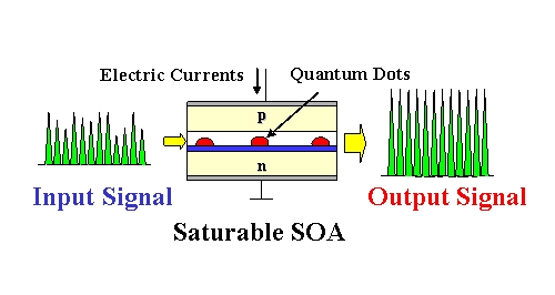
Fujitsu Limited and Fujitsu Laboratories Limited today announced the development of the world's first semiconductor optical amplifier (SOA)(1) enabling waveform re-shaping of high-speed optical signals at 40Gbps by using quantum dots(2). Optical technology capable of restoring degradation of optical signals to their original quality without converting them into electronic signals is known as all-optical 3R regeneration(3), consisting of re-amplification, re-shaping, and re-timing. The new SOA accomplishes both re-amplification and re-shaping of optical signals through a single semiconductor device, thereby enabling optical regenerators to become further compact and facilitating higher functionality of future optical networks.

New technology developed for this SOA will be the foundation for the realization of future ultra high-speed photonic networks. Research for this technology was partially conducted as part of the project "R&D of High Performance Network Subsystems Using Nano Technology", commissioned by the Ministry of Internal Affairs and Communications (MIC) of Japan.

Details of this development will be presented at the Optical Fiber Communication Conference (OFC) 2005, which starts March 6 in Anaheim, U.S.

Background

For future photonic networks that require high-speed optical signals to be transmitted at high qualities over long distances and flexible interconnect of optical network nodes, all-optical 3R regeneration is extremely effective. Optical 3R regeneration technology consists of three key processes: re-shaping, re-timing, and re-amplification. Re-shaping refers to the suppression of noise and fluctuation of optical signals to re-shape signal waveforms, re-timing reduces timing fluctuations know as timing jitter, and re-amplification amplifies optical signals.

In the past, as optical signals were regenerated by converting them into electronic signals and using electronic circuits for regeneration, optical regeneration required large and complex regenerators. Therefore, various research has been underway to develop all-optical regenerators capable of regenerating optical signals without requiring their conversion into electronic signals.

Technological Challenges

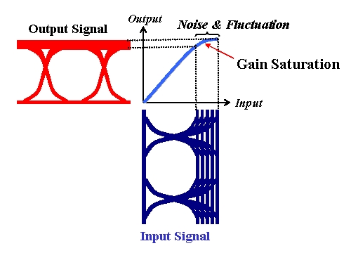
SOAs can suppress noise and fluctuation when optical signals are on (ON-level), by utilizing a characteristic known as gain saturation, in which the optical gain (amplification rate) falls when a signal is too intense. However, conventional SOAs typically had slow gain saturation response speeds requiring several nanoseconds, thereby impacting the subsequent signal and making such SOAs unusable in all-optical regenerators.

Newly Developed Technology

Technology that Fujitsu developed for its new SOA significantly accelerates the response speed of gain saturation. Fujitsu achieved this by observing and focusing on the extremely fast speeds of gain saturation when quantum dots were used. By employing quantum dots, gain saturation response time was accelerated to a few picoseconds, one-thousandth the time that was required with conventional SOAs.

In addition, through improvements in crystal growth technology of quantum dots(4) and by designing a new device structure, Fujitsu realized a quantum dot SOA which easily enables gain saturation while achieving high optical gain and high optical output, at wavelengths of 1550 nanometers (nm) which are used in optical telecommunication

Results

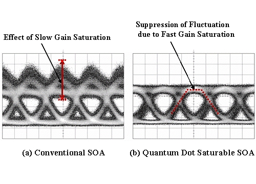
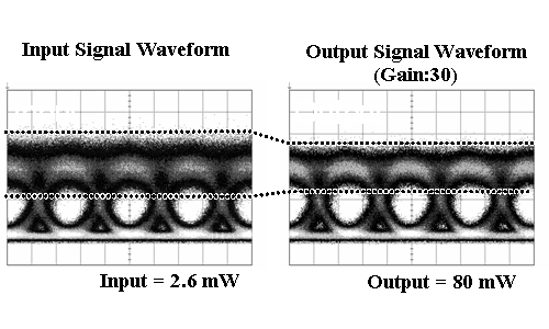
By using its new SOA, Fujitsu achieved the world's first successful waveform re-shaping and suppression of fluctuations of high-speed optical signals at 40Gbps. Unlike conventional SOAs in which waveform degradation occurred due to slow response time, such waveform degradation is not observed with Fujitsu's new SOA that employs quantum dots. By intentionally adding noise to the input signal, Fujitsu also succeeded in significantly suppressing output signal noise. When the input signal was amplified by 30 times (15 decibels), the noise to signal ratio was reduced by 40%.

Future Developments

Fujitsu will further optimize this new SOA and continue with development of a function to suppress fluctuations when signals are off (OFF-level fluctuations), and a re-timing function. Fujitsu targets the realization of an all-optical 3R regenerator using practical technology in the next four or five years. Fujitsu will also hereafter consider employing its new SOA for wavelength division multiplexing (WDM) applications.

Quantum dot SOA and input/output signal waveformsFigure 1. Quantum dot SOA and input/output signal waveforms


Diagram of the principle of re-shaping (suppression of noise: ON-level fluctuation)Figure 2. Diagram of the principle of re-shaping (suppression of noise: ON-level fluctuation) using gain saturation


Comparison of output waveform between a conventional SOA and Fujitsu's newly developed quantum dot SOA (Signal wavelength: 1550nm, signal transfer speed: 40Gpbs)Figure 3. Comparison of output waveform between a conventional SOA and Fujitsu's newly developed quantum dot SOA (Signal wavelength: 1550nm, signal transfer speed: 40Gpbs)


Effect of noise (ON-level fluctuation) suppression (re-shaping) using a quantum dot SOA (Signal wavelength: 1550nm, signal transfer speed: 40Gbps)Figure 4. Effect of noise (ON-level fluctuation) suppression (re-shaping) using a quantum dot SOA (Signal wavelength: 1550nm, signal transfer speed: 40Gbps)

  • [1] semiconductor optical amplifier (SOA)

    A semiconductor device that amplifies an optical signal through the stimulated emission of stored carriers in a semiconductor. The carriers are usually supplied by electrical current.

  • [2] quantum dots

    Nano-scale semiconductors consisting of semiconductor crystals that are several dozen nanometers in size, in which electrons can be stored.

  • [3] all-optical 3R regeneration

    Optical 3R regeneration is technology whereby a degraded signal is restored to its original quality, and consists of Re-amplification, Re-timing, and Re-shaping (3R). When these processes do not involve conversion to electronic signals, they are referred to as all-optical 3R regeneration.

  • [4] improvements in crystal growth technology of quantum dots

    Fujitsu utilized and modified technology based on research results from "InAs Quantum Dot Growth Technology on InP Substrates", which was conducted as part of the Photonic Network Project of the Optoelectric Industry and Technology Development Association (OITDA), commissioned by the New Energy and Industrial Technology Development Organization (NEDO) of Japan.

About Fujitsu

Fujitsu is a leading provider of customer-focused IT and communications solutions for the global marketplace. Pace-setting technologies, highly reliable computing and communications platforms, and a worldwide corps of systems and services experts uniquely position Fujitsu to deliver comprehensive solutions that open up infinite possibilities for its customers' success. Headquartered in Tokyo, Fujitsu Limited (TSE: 6702) reported consolidated revenues of 4.7 trillion yen (US$45 billion) for the fiscal year ended March 31, 2004.
For more information, please see: http://www.fujitsu.com/

About Fujitsu Laboratories

Founded in 1968 as a wholly owned subsidiary of Fujitsu Limited, Fujitsu Laboratories Limited is one of the premier research centers in the world. With a global network of laboratories in Japan, China, the United States and Europe, the organization conducts a wide range of basic and applied research in the areas of Multimedia, Personal Systems, Network, Peripherals, Advanced Materials and Electronic Devices. For more information, please see: http://jp.fujitsu.com/labs/en/

Press Contacts

Public and Investor Relations
Inquiries

Company:Fujitsu Limited

Technical Contacts

Photonics and Electronics Laboratories
Optical Semiconductor Devices Lab.

Phone: Phone: +81-46-250-8250
E-mail: E-mail: optisemi@ml.labs.fujitsu.com
Company:Fujitsu Laboratories Ltd.


All company and product names mentioned herein are trademarks or registered trademarks of their respective companies.

Date: 04 March, 2005
City: Tokyo
Company: Fujitsu Limited, Fujitsu Laboratories Ltd., , , ,