Tokyo and Kawasaki, Japan, September 08, 2015
Fujitsu Limited and Fujitsu Laboratories Ltd. today announced the development of the world's first 300 GHz band compact receiver capable of high-speed wireless communications at a rate of several tens of gigabits per second.
Radio signals with a frequency greater than 100GHz, called the terahertz band, allow for increases in usable frequency range and communication speed of more than 100 times compared with the 0.8-2.0 GHz range used by current mobile devices.
Now, Fujitsu has developed technology that combines a receiver-amplifier chip and terahertz-band antenna with a low-loss connection. This has made it possible to reduce the receiver's size to one tenth that of previous receivers, making use in mobile devices possible.
A portion of these research results were obtained through "R&D Program on Multi-tens Gigabit Wireless Communication Technology at Subterahertz Frequencies," a research program commissioned by Japan's Ministry of Internal Affairs and Communications as part of its "Research and Development Project for Expansion of Radio Spectrum Resources."
Details of this technology will be presented at European Microwave Week (EuMW) 2015, the international conference to be held beginning Sunday, September 6, in Paris, France.
Development Background
High-volume data communications such as video and music downloads are widely used on mobile devices such as smartphones and tablets. With an anticipated shift to high-volume data communications, such as 4K and 8K HD video and high-resolution audio sources, there will be an increasing need for near-instantaneous downloads (Fig. 1). This makes a speed increase in wireless communication devices necessary. Such devices that use the terahertz band, or frequencies over 100 GHz, are able to increase both the range of useable frequencies and the speed of communications by over 100 times of those used in current mobile terminals.
On the other hand, as terahertz-band waves attenuate sharply when propagating through space, a highly sensitive receiver is necessary to receive data from weak waves. In recent years, highly sensitive receiver-amplifier chips that work in the terahertz band have been developed by a number of companies, but with the necessity to make the module that mounted the receiver-amplifier chip and the exterior antenna separately, the receivers produced were large and difficult to integrate into mobile devices.
 Figure 1: Using a terahertz-band high-sensitivity receiver
Issues
Existing high-sensitivity terahertz-band receivers consist of a receiver-amplifier module and separate antenna, with a specialized component called a waveguide to connect them, which makes for large receivers. The most effective way to miniaturize them is to build the antenna directly into the receiver-amplifier module and eliminate the waveguide. Modules with built-in antennas are built by connecting the antenna and the receiver-amplifier chip through an internal printed-circuit substrate, making a waveguide unnecessary. The problem then is that the most common materials for printed-circuit substrates for high-frequency waves are ceramic, quartz, or Teflon, but when used in the terahertz band, there is significant signal attenuation and loss of receiving sensitivity.
Newly Developed Technology
By developing a low-loss technology for connecting terahertz-band antennas with already developed receiver-amplifier chips, Fujitsu has now developed the world's first 300 GHz band receiver with an internal antenna. With a cubic capacity at 0.75 of a centimeter (not including output terminals) it can be installed in mobile devices.
Below are the features of the newly developed technology:
- Uses a low-loss polyimide that can be micro-fabricated into printed-circuit boards
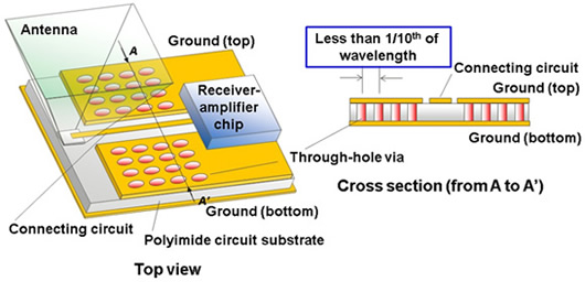
Fujitsu used a polyimide that can be micro-fabricated for the printed-circuit substrate. Signals received by the antenna are transmitted to the receiver-amplifier chip through a connecting circuit. In order to ensure that the terahertz signal is transmitted through the connecting circuit dependably, with low loss, the top and bottom layers of the printed-circuit substrate are grounded, and these layers are connected with electrical lines called through-hole vias. These vias need to be spaced apart by less than one-tenth of the signal's wavelength-in this case, less than a few tens of microns-in order for the radio waves to be transmitted properly. While polyimide as a material has a 10% higher loss than quartz, because its processing accuracy is more than four times higher, the through-hole vias can be placed within several tens of microns of each other, halving the loss as compared to a connecting circuit on a quartz printed circuit (fig. 2).
 Figure 2: Internal construction of the terahertz-band high-sensitivity receiver (the connection between the internal antenna and the receiver-amplifier chip)
- Establishes mounting technology for terahertz-band receiver-amplifier chips
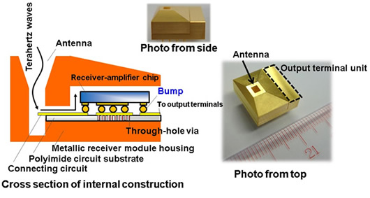
In order to transmit the received signal from the connecting circuit on the printed-circuit substrate to the receiver-amplifier chip with low loss, Fujitsu developed mounting technology that faces the circuit-forming surface of the receiver-amplifier chip toward the printed-circuit substrate. This mounting technology is used for mounting millimeter-wave band collision-avoidance radar chips, but by using it with the polyimide circuit substrate-based low loss transmission technology mentioned above, Fujitsu has successfully expanded the applicable frequencies into the terahertz band for the first time (fig. 3).
 Figure 3: The terahertz-band high-sensitivity receiver and a cross section of its construction (cross section of receiver-amplifier chip mounting)
Results
With mobile devices such as smartphones capable of high-volume communication at rates of several tens of gigabits per second, the use of this Fujitsu-developed technology will enable small devices to receive 4K or 8K HD video instantly, such as from a download kiosk with a multi-gigabit connection. It will also be possible to expand into such applications as split-second data transfers between mobile devices and split-second backup between mobile devices and servers.
Future Plans
In fiscal 2015, Fujitsu and Fujitsu Laboratories will begin field trials of multi-gigabit-per-second, high-speed data transfer using this newly developed compact receiver, aiming to commercialize this technology around 2020.
![]() E-mail: tera@ml.labs.fujitsu.com
E-mail: tera@ml.labs.fujitsu.com

