Fujitsu

Global

Archived content

NOTE: this is an archived page and the content is likely to be out of date.

Fujitsu, PETRA, and NEDO Achieve World's Lowest Energy Requirements of 5 mW per 1 Gbps for High-Speed Inter-Processor Data Transmissions

Silicon photonics technology used to successfully halve power requirements

Fujitsu Limited,Fujitsu Laboratories Ltd.,Fujitsu Laboratories of America Inc.,Photonics Electronics Technology Research Association,New Energy and Industrial Technology Development Organization
Tokyo and Kawasaki, Japan, and Sunnyvale, CA, February 23, 2015

Fujitsu Limited, Fujitsu Laboratories Ltd., Fujitsu Laboratories of America, Inc., the Photonics Electronics Technology Research Association (PETRA), and the New Energy and Industrial Technology Development Organization (NEDO) today announced that they have jointly developed the world's most energy-efficient silicon photonics(1) optical transceiver circuit for high-speed data transmissions between CPUs in servers and supercomputers, requiring only 5 mW of electricity per 1 Gbps(2) of transmission speed.
Optical devices have needed a certain amount of voltage in order to run at high speeds, making it difficult to reduce the power needed for optical transceiver circuits. Now Fujitsu and its partners have developed a technology that allows optical devices to be run at a low voltage by significantly increasing amplitude when there is a change in the data being transmitted, resulting in high-speed operations of 25 Gbps at half the power previously required.

While reducing the amount of power consumed, this technology enables multiple optical transceiver circuits to run in parallel for high-speed, terabit-class transmissions, and is therefore expected to raise the performance of servers and supercomputers.

Parts of this technology were developed in the "Integrated Photonics-Electronics Convergence System Technology (PECST)" project that NEDO entrusted to PETRA, while Fujitsu Limited, Fujitsu Laboratories, and Fujitsu Laboratories of America are collaborating to develop the transceiver circuit technology.

Details of this technology are being presented at IEEE International Solid-State Circuits Conference 2015 (ISSCC 2015), the foremost global forum for solid-state circuits, opening February 22 in San Francisco (ISSCC presentation 22.2).

Background

With large-scale system servers and supercomputers that possess multiple connected CPUs, the volume of data transmitted within and between CPU-equipped units continues to rise as performance levels increase. Improving the performance of servers and supercomputers, therefore, requires not just raising the calculating performance of each individual CPU, but also raising the speed of data transmissions between connected CPUs. Overall systems for servers and supercomputers require significant amounts of power, but due to constraints on the amount of power facilities can supply, there is a desire to increase the data transmission speeds of transceiver circuits without increasing the amount of power consumed.

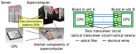
For silicon photonics-based optical transceiver technology, which holds significant promise for the next generation of high-performance supercomputers, optical devices are effectively limited to transmission speeds of 25 Gbps. One way of increasing overall transmission speeds is to run in parallel multiple optical devices and the electronic circuitry of their optical transceiver circuits. There is a need to double the speed of data transmissions between CPUs in four years. So to achieve this doubling while holding power constant, the power consumed by optical transceiver circuits needs to be cut in half (Figure 1).

Figure 1: Inter-processor data communications in high-performance servers and supercomputersFigure 1: Inter-processor data communications in high-performance servers and supercomputers

Technological Issues

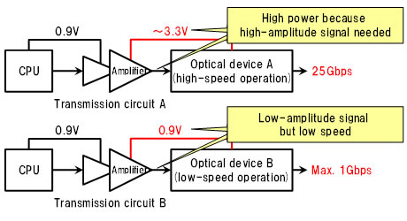
Typically, with high-speed, 25 Gbps optical transmissions, optical devices operate at 3 volts (V) or higher, compared to the 0.9 V that CPUs and other electronic circuits need. Because transmission circuits that drive optical devices also operate at higher voltages in order to constantly send high-amplitude signals to the optical devices for high-speed operations, reducing their power consumption has proven difficult. Conversely, if optical devices operating at 0.9 V, the same low voltage as the CPU, were employed to consume less power, only a problematically low-speed operation of around 1 Gbps could be achieved (Figure 2).

Figure 2: Issues with optical transceiver circuitsFigure 2: Issues with optical transceiver circuits

About the Technology

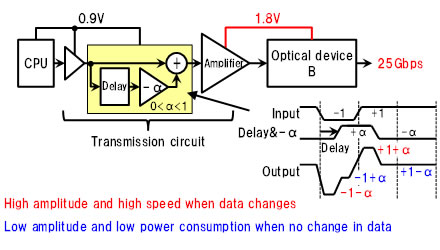
Now, by amplifying the transmission signal only when the signal from the CPU changes to -1 and +1, the researchers on this project succeeded at generating amplitudes intermittently at around 1.8 V. As a result, the supplied voltage is 1.8 V, lower than the 3.3 V previously required, and because power is not used with smaller amplitudes when the data do not change, less power is consumed.

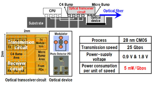
The principal behind this technology is that the data being transmitted is combined with delayed data that is multiplied by -α (where 0 < α < 1), so that when the transmission data changes from -1 to +1, +1 is amplified to +1+α. On the other hand, when the transmission data changes from +1 to -1, -1 can be amplified further to -1-α (Figure 3). This technology enables both higher speeds and lower power consumption, and the researchers on the project confirmed that they could achieve high-speed transmissions of 25 Gbps while operating at half the power previously required, achieving operation of 5 mW of electricity per 1 Gbps of transmission speed (Figure 4).

Figure 3: How this technology achieves high speed and low power consumptionFigure 3: How this technology achieves high speed and low power consumption

Figure 4: Schematic, photo, and specifications of the new optical transceiver chipFigure 4: Schematic, photo, and specifications of the new optical transceiver chip

Results

While reducing the amount of power consumed, this technology enables multiple optical transceiver circuits to run in parallel for high-speed, terabit-class transmissions, and is therefore expected to raise the performance of servers and supercomputers.

Future Plans

Fujitsu Laboratories is applying this technology to the interfaces of CPUs and optical modules, and aims for practical implementations in fiscal 2018. The company is also studying applications in the next generation of high-performance servers and supercomputers.


  • [1] Silicon photonics

    Technology in which an optical device is configured on a silicon substrate. By using silicon, optical circuits can be made smaller, enabling large-scale integration. It also has other merits, such as the ability to configure optical circuits and electronic circuits in one unit, and lower manufacturing costs.

  • [2] Gbps

    Gigabits (billion bits) per second.

About Fujitsu

Fujitsu is the leading Japanese information and communication technology (ICT) company offering a full range of technology products, solutions and services. Approximately 162,000 Fujitsu people support customers in more than 100 countries. We use our experience and the power of ICT to shape the future of society with our customers. Fujitsu Limited (TSE: 6702) reported consolidated revenues of 4.8 trillion yen (US$46 billion) for the fiscal year ended March 31, 2014. For more information, please see http://www.fujitsu.com.

About Fujitsu Laboratories

Founded in 1968 as a wholly owned subsidiary of Fujitsu Limited, Fujitsu Laboratories Ltd. is one of the premier research centers in the world. With a global network of laboratories in Japan, China, the United States and Europe, the organization conducts a wide range of basic and applied research in the areas of Next-generation Services, Computer Servers, Networks, Electronic Devices and Advanced Materials. For more information, please see: http://www.fujitsu.com/jp/group/labs/en/.

About Fujitsu Laboratories of America

Fujitsu Laboratories of America, Inc. is a wholly owned subsidiary of Fujitsu Laboratories Ltd. (Japan), focusing on research on Internet, interconnect technologies, software development and solutions for several industry verticals. Conducting research in an open environment, it contributes to the global research community and the IT industry. It is headquartered in Sunnyvale, CA.
For more information, please see: http://www.fla.fujitsu.com

About PETRA

PETRA is a research association in JAPAN for developing innovative technologies in Photonics-Electronics convergence system.
PETRA was established in 2009, and consists of 11 companies, 1 National Laboratory and 1 Association.

About NEDO

Following its establishment as a semi-governmental organization in 1980, the New Energy and Industrial Technology Development Organization (NEDO) is Japan's largest public research and development management organization. NEDO undertakes technology development and demonstration activities to carry out two basic missions, addressing energy and global environmental issues and enhancing industrial technology, by integrating the combined efforts of industry, academia, and government.
Press Contacts

Public and Investor Relations Division
Inquiries

Company:Fujitsu Limited

Technical Contacts

ICT Systems Laboratories
Server Technologies Lab


E-mail: E-mail: SiPh_ISSCC2015@ml.labs.fujitsu.com
Company:Fujitsu Laboratories Ltd.


All company or product names mentioned herein are trademarks or registered trademarks of their respective owners. Information provided in this press release is accurate at time of publication and is subject to change without advance notice.

Date: 23 February, 2015
City: Tokyo and Kawasaki, Japan, and Sunnyvale, CA
Company: Fujitsu Limited, Fujitsu Laboratories Ltd., Fujitsu Laboratories of America Inc., Photonics Electronics Technology Research Association, New Energy and Industrial Technology Development Organization