![]()
Archived content
NOTE: this is an archived page and the content is likely to be out of date.
Fujitsu Develops New Packaging Technology Enabling 90% Power Combining Efficiency
77-Ghz band CMOS amplifiers achieve 32mW output—will contribute to low-cost, compact transceivers for vehicle-mounted radar and wireless communications devices
Fujitsu Laboratories Ltd.
Fujitsu Laboratories today announced the development of a new packaging technology that enables the development of millimeter-wave(1) power amplifiers that can be employed in applications such as automotive radar(2) and wireless communications devices.
One effective way to produce compact, low-cost millimeter-wave transceivers is to integrate high-frequency RF circuitry onto a CMOS(3) chip. At the same time, for normal CMOS circuitry, which operates at low voltages, the high power amplifiers employed in transmitters has proven a challenge that has served as a roadblock to integration. As a result, there has been a need for a technology that can enable CMOS power amplifiers to achieve higher output.
Fujitsu Laboratories has developed a technology that combines millimeter-wave high-frequency signals generated by multiple power amplifiers within an off-chip module. A prototype module incorporating CMOS power amplifiers based on this technology was able to produce 32 mW output in the 77-GHz frequency band. As a result, it will become possible to develop CMOS millimeter-wave transceivers that employ high-output power amplifiers, which is expected to substantially contribute to the production of smaller, low-cost devices.
Details of the technology will be presented at the European Microwave Conference 2012, to be held beginning October 28, 2012 in the Netherlands.
Background
In recent years, there has been a widespread adoption of applications employing millimeter-wave technology, such as 77-GHz band automotive radar and 60-GHz band high-capacity wireless communications devices. The RF transceiver ICs presently used in these applications are compound semiconductors(4), which have superior high-frequency characteristics. On the other hand, recent advances in process technologies have brought the operational speed of CMOS technology up to par with that of compound semiconductors, and research is being conducted on ways to implement RF circuitry in CMOS, which can be cheaply manufactured in mass quantities, rather than in compound semiconductors.
Technological Issues
The challenge involved in integrating an RF transceiver into a CMOS chip is in increasing the output of the power amplifier employed in the transmitter. Advances in miniaturization cause a decrease in the power-supply voltages of CMOS circuits, thereby making it difficult to implement high-output power amplifiers. This, in turn, has stood in the way of obtaining power outputs on par with compound semiconductors.
One well-known way to achieve high output from power amplifiers is to array several in parallel and combine their output. If this combining circuitry is fabricated using CMOS on-chip interconnects (see Figure 1a), the thinness of the wiring results in significant line resistance and the power output from the power amplifier is attenuated by roughly 30% by the time it reaches the transmitter, resulting in reduced efficiency. Conversely, if the combining circuit is fabricated on a typical printed-circuit board used in electronic devices (see Figure 1b), the transmission of millimeter-wave signals is impaired due to difficulties in interconnect miniaturization, and the increased size of the module containing the power amplifiers becomes problematic. Therefore, a compact, efficient power combination circuit is desired.
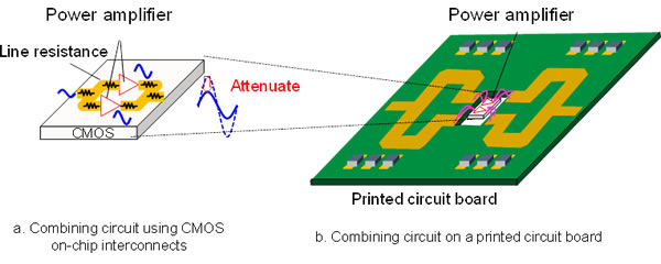 Figure 1: Conventional power amplifier combining circuitry
About the New Technology
Fujitsu Laboratories has developed a new packaging technology (redistribution layer, or RDL, technology) that combines millimeter-wave high-frequency signals generated by power amplifiers within an off-chip module. This, in turn, has enabled the construction of higher output millimeter-wave power amplifiers.
Redistribution layer technology is a packaging technique for semiconductor components in which chip-level semiconductor elements are reconfigured as wafers using a mold compound (Figure 2a) and subsequently formed into a package that connects the electrode patterns between chips through an interconnect process. As the interconnects are formed using a wafer process, fine patterns can be achieved.
As shown in the cross-sectional view in Figure 2b, a variety of different devices, such as the chip capacitors, can be integrated in the same package, and components can be assembled with high density. Packaging technology using a single-layered RDL has been developed as compact packaging technology for use in applications such as mobile phones, but a packaging structure suited to transmitting millimeter-wave signals has not been developed.
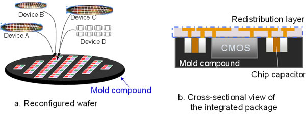 Figure 2: Integrated package using redistribution layer
To enable the transmission of high-frequency millimeter-wave signals, Fujitsu Laboratories has developed a power combining circuit that employs multi-layer interconnect technology using multiple interconnection layers (see Figure 3a). As shown in Figure 3b, the interconnection layer formed using an RDL can be more than five times as thick as a typical CMOS on-chip interconnect, thereby reducing line resistance and minimizing losses in the combining circuitry. In addition, by optimizing the thickness of insulation films and the width of interconnect patterns, Fujitsu Laboratories developed a combining circuit that reduces signal loss to less than 10%.
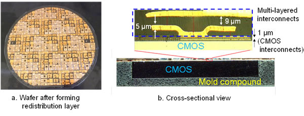 Figure 3: Cross-sectional comparison of CMOS on-chip interconnect with RDL
By adopting this combining circuit in a CMOS power amplifier, it was possible to develop a high-output power amplifier module (see Figure 4). Power output comes from four CMOS power amplifiers arrayed in parallel that each produce 9 mW at 77 GHz, which is channeled to a combining circuit formed using RDL technology. Reducing power loss to 10%—compared to 30% via existing techniques—meant the technology achieved a power combining efficiency of 90%, with power output of 32 mW.
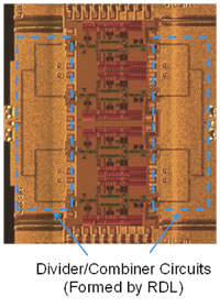 Figure 4: Photo of power amplifier module using RDL technology
Results
Fujitsu Laboratories has developed a packaging technology that combines CMOS and RDL technology to increase the power output of power amplifiers. By enabling the implementation of power amplifiers on a CMOS chip, which was previously problematic, it will be possible to implement all millimeter-wave RF circuits in CMOS. This is expected to lead to smaller, low-cost RF transceiver chips, as well as low-cost millimeter-wave applications.
Future Plans
Fujitsu Laboratories plans to expand the use of this technology beyond power amplifiers to a wide range of millimeter-wave RF circuitry connections, while working to develop inexpensive, compact wireless communications modules.
-
[1] Millimeter-wave
Electromagnetic spectrum between the wavelengths of 1–10 mm (frequencies of 30–300 GHz).
-
[2] Automotive radar
A system that measures the distance, direction, and relative speed of other vehicles using outgoing and incoming radio signals.
-
[3] CMOS technology
A logic circuit consisting of N-type and P-type metal-oxide semiconductors (MOS) with complementary connections formed on a silicon substrate. Attributable to their low power requirements, CMOS circuits are currently the mainstream for integrated circuits.
-
[4] Compound semiconductor
A semiconductor formed using two or more elements, such as gallium-arsenide (GaAs) or indium-phosphide (InP), and which features higher electron mobility than silicon, therefore permitting faster operation.
About Fujitsu
Fujitsu is the leading Japanese information and communication technology (ICT) company offering a full range of technology products, solutions and services. Over 170,000 Fujitsu people support customers in more than 100 countries. We use our experience and the power of ICT to shape the future of society with our customers. Fujitsu Limited (TSE:6702) reported consolidated revenues of 4.5 trillion yen (US$54 billion) for the fiscal year ended March 31, 2012. For more information, please see http://www.fujitsu.com.
About Fujitsu Laboratories
Founded in 1968 as a wholly owned subsidiary of Fujitsu Limited, Fujitsu Laboratories Limited is one of the premier research centers in the world. With a global network of laboratories in Japan, China, the United States and Europe, the organization conducts a wide range of basic and applied research in the areas of Next-generation Services, Computer Servers, Networks, Electronic Devices and Advanced Materials. For more information, please see: http://jp.fujitsu.com/labs/en.
Technical Contacts
Device & Materials Laboratories
![]() E-mail: cmos_rdl@ml.labs.fujitsu.com
E-mail: cmos_rdl@ml.labs.fujitsu.com
Company:Fujitsu Laboratories Ltd.
All company or product names mentioned herein are trademarks or registered trademarks of their respective owners. Information provided in this press release is accurate at time of publication and is subject to change without advance notice.
Date: 29 October, 2012
City: Kawasaki, Japan
Company:
Fujitsu Laboratories Ltd.,
,
,
,
,
,
,
,
,
,