![]()
Archived content
NOTE: this is an archived page and the content is likely to be out of date.
Fujitsu Develops Analog-to-Digital Converter that Reduces Die Area and Cuts Power Consumption by Half
Contributes to More Compact and Power-efficient Digital Systems
Fujitsu Laboratories Ltd.
Fujitsu Laboratories today announced that it has developed an analog-to-digital converter (ADC) that is 50% smaller and consumes 50% less power than conventional converters.
A typical ADC works by comparing the voltage of an external analog input signal with an internally generated reference level to convert to a digital value. Switches are required to change the reference levels, however, advancements in semiconductor process scaling have made it difficult to guarantee high-speed switching.
To overcome these issues, Fujitsu Laboratories has developed a completely new circuit design by using digital control techniques that require neither the use of a switch nor the generation of a reference voltage.
Using this design, Fujitsu Laboratories developed an ADC with 6-bit resolution and a conversion rate of 1 Giga Sample per second (GS/s) that has a die area of 0.04mm2—the world's smallest for that performance class—and that consumes 9.9mW of electricity. In addition, by using multi-channel time-interleaved operation(1) to enable high-speed operation, performance levels of several tens of GS/s can be achieved, contributing to major performance enhancements in the systems in which it is installed.
Details of this technology were published at the 2012 International Symposium on VLSI Design, Automation & Test (2012 VSLI-DAT), which was held in Taiwan from Monday, April 23.
Background
Recent advancements in digital equipment have mainly been realized by performance improvements in digital circuits. Information and signals in the natural world, however, exist as analog form, and therefore require an ADC to convert them into digital form for digital processing.
In addition, even if the signals are in digital form, such as is the case with a hard disk drive (HDD), when signals are transmitted at high speeds and high densities, they are distorted, making it difficult to read the original digital value. Therefore, it is becoming increasingly common now to apply digital signal processing to resolve the original digital values by converting the distorted digital signal into digitized value (Figure 1).
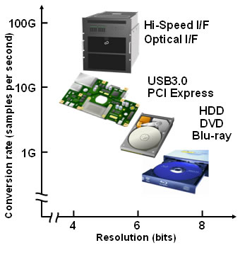 Figure 1: ADC Performance and Areas of Application
Technological Issues
A typical ADC works by comparing the voltage of an external analog input signal with internally generated reference voltage levels to convert the analog input signal into digital level(Figure 2). To generate the reference voltages, however, a resistor ladder for reference voltages is required, which dissipates static current. In addition, to implement the reference voltage levels, switches are needed, and advancements in semiconductor process scaling have made it increasingly difficult to guarantee high-speed switching performance, because of wide variation of switch on-resistance.
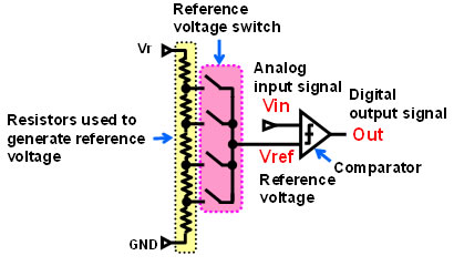 Figure 2: Conventional ADC
Fujitsu's Newly Developed Technology
Fujitsu Laboratories has developed a completely new circuit design based on a digital control technique that requires neither the use of resistors to generate reference voltage levels nor switches for switching reference voltage levels. Instead of using a reference voltage, it uses a digitally controlled threshold level. It works by comparing whether the analog input signal is bigger or smaller than a threshold level controlled digitally (Figure 3). Specifically, the quantized units of current sources are arranged in the comparator, and by adjusting the number of current units, the threshold level is controlled (Figure 4).
By using this configuration, there is no need for the resistors to generate the reference voltage levels, thus eliminating the need for the static current used in the resistors (roughly 1mA). Moreover, because there is no need for a reference voltage switch, higher operation speed can be achieved.
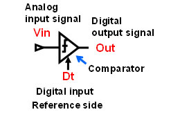 Figure 3: Newly Developed ADC
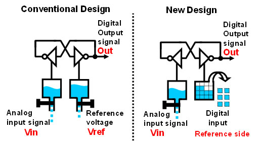 Figure 4: Comparison of the Internal Structure of the Comparators
Using this design technique, Fujitsu Laboratories developed a prototype ADC with 6-bit resolution and a conversion rate of 1 GS/s that has a die area of 0.04mm2—the world's smallest for that performance class—and that consumes just 9.9mW.
Results
This new design reduces the die area and cuts the power consumption by 50% compared to conventional ADCs. This enables compactness and high energy efficiency, even with time-interleaved operations that achieve high-speed performance of several tens of Giga Samples per second (GS/s) in multi-channel time interleaved operation, contributing to major performance enhancements in the systems in which they are deployed.
Future Plans
Fujitsu plans to apply this technology in various ways, including to the backplane interfaces between circuit boards in servers. In addition, while working on applications involving further process scaling, Fujitsu also plans to apply the technology to other analog circuits.
-
[1] Time-interleaved operation
A technology designed to achieve higher-speed operation by phase shifting operations in circuits over multiple channels.
About Fujitsu
Fujitsu is the leading Japanese information and communication technology (ICT) company offering a full range of technology products, solutions and services. Over 170,000 Fujitsu people support customers in more than 100 countries. We use our experience and the power of ICT to shape the future of society with our customers. Fujitsu Limited (TSE:6702) reported consolidated revenues of 4.5 trillion yen (US$55 billion) for the fiscal year ended March 31, 2011. For more information, please see http://www.fujitsu.com
About Fujitsu Laboratories
Founded in 1968 as a wholly owned subsidiary of Fujitsu Limited, Fujitsu Laboratories Limited is one of the premier research centers in the world. With a global network of laboratories in Japan, China, the United States and Europe, the organization conducts a wide range of basic and applied research in the areas of Next-generation Services, Computer Servers, Networks, Electronic Devices and Advanced Materials. For more information, please see: http://jp.fujitsu.com/labs/en.
Technical Contacts
Platform Technologies Laboratories
![]() E-mail: hsadc@ml.labs.fujitsu.com
E-mail: hsadc@ml.labs.fujitsu.com
Company:Fujitsu Laboratories Ltd.
All other company or product names mentioned herein are trademarks or registered trademarks of their respective owners. Information provided in this press release is accurate at time of publication and is subject to change without advance notice.
Date: 23 April, 2012
City: Kawasaki, Japan
Company:
Fujitsu Laboratories Ltd.,
,
,
,
,
,
,
,
,
,