![]()
Archived content
NOTE: this is an archived page and the content is likely to be out of date.
Fujitsu Develops World's Highest-Performance Ultra-Low-Noise Transistor for Millimeter-Band Receivers
Reduces image capture time of image sensors by half; helps to close the digital divide
Fujitsu Limited,Fujitsu Laboratories Ltd.
Fujitsu Limited and Fujitsu Laboratories Ltd. today announced the development of an indium phosphide-based high electron mobility transistor (InP HEMT)(1) using their proprietary "space cavity" structure that, operating at the millimeter-band frequency level of 94 GHz(2), reduces the noise level generated by the transistor by approximately 30% compared to previous technologies(3), to 0.7 decibels, resulting in the world's lowest noise levels. The novel noise-lowering technology will enable sensitivity enhancements in millimeter-band receivers, which in turn would enable the time required for image capture by image sensors(4) - being deployed for anti-terrorist initiatives in major airports - to be reduced by nearly half. In addition, as the new technology can enable range extension by 20% of high-capacity wireless transmission distance on par with optical transmissions, wireless networks can be used in place of trunk lines in locations where it is difficult to install fiber-optic cabling, thereby helping to close the digital divide(5).
Part of this research was conducted under contract as part of the Research and Development Project for Expansion of Radio Spectrum Resources of Japan's Ministry of Internal Affairs and Communications. Details of this technology will be presented at the 22nd International Conference on Indium Phosphide and Related Materials (IPRM 2010), held May 31 - June 4 in the city of Takamatsu, located in Japan's Kagawa Prefecture.
Background
In contrast to infra-red or optical signals, radio waves in the millimeter-band frequency range - which extends from 30 GHz to 300 GHz - are permeable and able to travel through thin walls and fabric. As part of their anti-terrorism prevention efforts, major airports around the world are considering deployment of image sensors that take advantage of the permeability of millimeter-waves.
Furthermore, as commercial use of wireless networks is limited and thus makes it easy to secure large swaths of bandwidth, millimeter-wave signals are ideal for transmitting very large volumes of data exceeding several gigabits per second. High-capacity millimeter-band transmission equipment can be used in place of trunk lines in locations where it is difficult to install fiber-optic cabling, making such equipment also useful in helping to close the digital divide. (Figure 1)
Image sensors must be able to detect very weak millimeter-waves emitted by people or objects, and high-capacity millimeter-band transceiver equipment needs to be able to detect signals that have weakened in the process of being transmitted and dispersed through the air. Thus, for both of these applications there is a need for high-sensitivity millimeter-band transceivers that can receive very weak millimeter-wave signals.
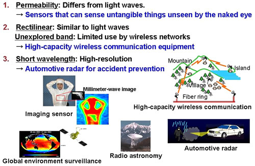 Figure 1: Features and applications of millimeter-waves
Larger View (127 KB)
Technological Challenges
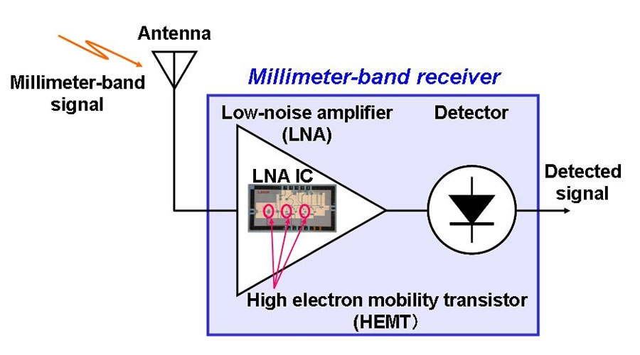
To make a millimeter-band transceiver highly sensitive (Figure 2), in the high electron mobility transistor (HEMT) that is used in the transceiver's amplifier, it is necessary to control the noise that is generated along with high signal amplification rates. If the noise level within the HEMT is high, the noise interferes with reception, thus making detection of weak signals impossible.
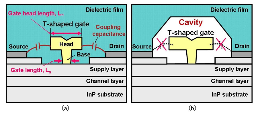
Thus far, in order to achieve high signal amplification rates with low noise, the conventional method used was to miniaturize the HEMT (see Figure 3a). However, miniaturizing the HEMT requires specialized fabrication equipment, and progress was limited due to low yields and poor uniformity. Therefore, the challenge was to find an alternative method for achieving high signal amplification rates with low noise.
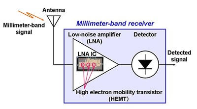 Figure 2: Structure of Fujitsu's millimeter-band receiver
Larger View (54 KB)
Newly-Developed Technology
Based on an analysis of the mechanisms by which noise is generated, Fujitsu developed novel technology to reduce noise. Key features of the new technology are as outlined below:
1) Employing a "space cavity" structure in the InP HEMT
In conventional InP HEMTs, if the coupling capacitance between the gate and the source or drain is large, a problem arises in that the millimeter-band signal amplification rates fall. To resolve this problem, Fujitsu eliminated the inter-layer dielectric film around the gate electrode, forming instead a "space cavity" that reduces the coupling capacitance. This technology was developed under a research contract from Japan's Ministry of Internal Affairs and Communications with the objective of increasing the speed of InP HEMTs, and for the first time ever, Fujitsu verified that reducing the coupling capacitance through the introduction of this "space cavity" structure has the added benefit of reducing noise.
2) Using a T-shaped gate(6) electrode to reduce gate resistance
Since the gate electrode on a HEMT is the source of noise, reducing gate resistance is an effective method for reducing noise. For that reason, HEMTs for lower frequencies that are used in transceivers for home satellite broadcast systems use a T-shaped gate, with a low-resistance head electrode placed on the upper part of a micro-electrode to reduce gate resistance and noise. However, when using a low-resistance T-shaped gate in the 94 GHz band, because the distance between the T-shaped gate and the source or drain is narrowed, there is an increase in noise from coupling capacitance. With the application of the "space cavity" structure, Fujitsu has now confirmed that even in the 94 GHz band, coupling capacitance is reduced when using the T-shaped gate. Moreover, Fujitsu also verified that increasing the length of the T-shaped gate's head also serves to reduce noise.
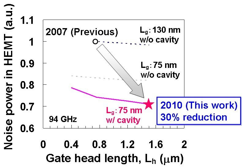
Employing the newly-developed technology, Fujitsu created an InP HEMT with a gate length of 75 nanometers(7) (see Figure 3b). As a result, Fujitsu succeeded in reducing noise within the transistor by 30% compared to previous technologies. The noise figure(8), which is a noise index for noise within the transistor, was reduced to 0.7 decibels, thus resulting in the world's lowest noise levels. (Figure 4)
Configuring an amplifier with the newly-developed HEMT greatly improves the sensitivity of millimeter-band receivers, holding the promise of reducing by half the time image sensors require for image capture and extending the transmission range of high-capacity millimeter-band transmission equipment by approximately 20%. As a result, security checks at airports would be much quicker, and wireless systems with date transmission capacities equivalent to optical transmission systems could be created, thereby accelerating the widespread deployment of millimeter-band systems that deliver speed and convenience in our daily lives.
 Figure 3: Cross-sectional views of conventional InP HEMT (a) and InP HEMT with "space cavity" (b)
Larger View (71 KB)
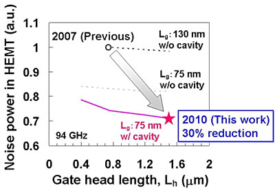 Figure 4: Effect of Fujitsu's newly-developed technology for reducing transistor noise (94GHz)
Larger View (65 KB)
Future Developments
Fujitsu plans to equip high-performance image sensors and high-capacity transmission equipment with amplifiers that will employ the newly-developed low-noise InP HEMT, targeting practical-use commercialization for 2012. Fujitsu will also strive to expand the range of applications into such areas as radio astronomy and the environmental monitoring of the earth.
-
[1] Indium-phosphide high electron-mobility transistor (InP HEMT)
Invented in 1979 by Fujitsu Laboratories researcher Takashi Mimura (currently a Fellow at Fujitsu Laboratories Ltd.), this is a transistor made of compound semiconductors featuring excellent speed and noise characteristics. Using an indium-phosphide (InP) substrate results in higher speed and lower noise than with conventional gallium-arsenide. This is considered useful in high-speed communications and millimeter-band image sensors.
-
[2] 94 GHz
Gigahertz (GHz) is a unit for measuring frequency, and 1 GHz equals 1 billion hertz. The 94 GHz band and 35 GHz band are currently used primarily in image sensors.
-
[3] Approximately 30% reduction compared to previous technologies
Compared to performance of InP HEMT technology announced by Fujitsu on June 7, 2007 (in Japanese only) and presented at International Microwave Symposium 2007 (IMS 2007).
-
[4] Image sensors
Pertaining to heat noise radiated by objects, image sensors are systems for capturing image data from objects by receiving millimeter-band (primarily 35 GHz band or 94 GHz band) signals in the form of heat radiated by objects.
-
[5] Digital divide
Refers to economic differences between those people or regions with good access to information and communications technology, versus those people or regions with poor access.
-
[6] T-shaped gate
A gate with an electrode in the shape of a "T" when viewed in cross-section. The base, which is the part touching the semiconductor, is made extremely narrow through miniaturization fabrication processes, enabling the transistor to operate at extremely high speeds, while the upper portion is thick to reduce total gate resistance, thereby combining the benefits of both high speed and low signal noise.
-
[7] Nanometer
A unit of length, with 1 nanometer (nm) equal to 1 one-millionth of a millimeter.
-
[8] Noise figure (NF)
The weakest input power level able to be used by an amplifier. When this value is small and a high signal amplification rate is used in the front-end of an amplifier, the impact of the noise figure after passing through the front-end is reduced, enabling receivers with sensitive signal reception.
About Fujitsu
Fujitsu is a leading provider of ICT-based business solutions for the global marketplace. With approximately 170,000 employees supporting customers in 70 countries, Fujitsu combines a worldwide corps of systems and services experts with highly reliable computing and communications products and advanced microelectronics to deliver added value to customers. Headquartered in Tokyo, Fujitsu Limited (TSE:6702) reported consolidated revenues of 4.6 trillion yen (US$50 billion) for the fiscal year ended March 31, 2010. For more information, please see: www.fujitsu.com.
About Fujitsu Laboratories
Founded in 1968 as a wholly owned subsidiary of Fujitsu Limited, Fujitsu Laboratories Limited is one of the premier research centers in the world. With a global network of laboratories in Japan, China, the United States and Europe, the organization conducts a wide range of basic and applied research in the areas of Next-generation Services, Computer Servers, Networks, Electronic Devices and Advanced Materials. For more information, please see: http://jp.fujitsu.com/labs/en.
Technical Contacts
![]() Phone: +81(46)250-8244
Phone: +81(46)250-8244
![]() E-mail: kikan-press@ml.labs.fujitsu.com
E-mail: kikan-press@ml.labs.fujitsu.com
Company:Fujitsu Laboratories Ltd.
Company and organization names mentioned herein are trademarks or registered trademarks of their respective owners. Information provided in this press release is accurate at time of publication and is subject to change without advance notice.
Date: 03 June, 2010
City: Tokyo and Kawasaki, Japan
Company:
Fujitsu Limited,
Fujitsu Laboratories Ltd.,
,
,
,