![]()
Archived content
NOTE: this is an archived page and the content is likely to be out of date.
Fujitsu Develops World's First 100 W-Class X-band High-Output Amplifier Featuring High Efficiency Exceeding 50%
- Also realizes world's highest C-band output at 343 W -
Fujitsu Laboratories Ltd.
Fujitsu Laboratories Limited today announced the development of the world's first 101-watt (101-W) X-band(1) high-output amplifier achieving the world's highest efficiency(2) of 53% using gallium nitride (GaN)(3)high electron-mobility transistors (HEMTs)(4). Compared to X-band amplifiers with same-class output power using gallium arsenide (GaAs) HEMTs, this new amplifier can save much power dissipation and can be expected to achieve twice the range. Furthermore, by employing the new amplifier in the C band(5), Fujitsu Laboratories achieved an output of 343 W, an advance over the 320 W output reported by Fujitsu Laboratories in 2008 which was the world's highest at that time. Compared to conventional amplifiers employing GaAs HEMTs, it is anticipated that this new GaN HEMT-based amplifier can achieve a range that is 2.6 times as great in the C band. This new amplifier technology holds the promise to serve as an alternative to traveling-wave tube amplifiers(6) in high-output applications, and may enable smaller, more energy-efficient, higher performance, and longer-lasting transmission systems in radars, satellite communications, and advanced mobile-phone base stations.
Details of this technology were presented at the 2009 IEEE MTT-S International Microwave Symposium (IMS2009) being held in Boston from June 7 to June 12.
Background
The microwave band - the range from 30 MHz to 30 GHz - is used for satellite communications, weather radar, and other applications. Microwave transmitters typically use high-output traveling-wave tube amplifiers or solid-state devices(7) with GaAs HEMTs. However, traveling-wave tube amplifiers have shorter life spans than solid-state devices and require extremely high-voltage power supply, thus making traveling-wave tube amplifiers heavy and bulky. Solid-state devices with GaAs HEMTs, on the other hand, have low output from individual transistor elements.
In 2008, Fujitsu Laboratories developed a C-band amplifier using GaN HEMTs, which has higher output electrical density and excellent dissipation characteristics compared to GaAs HEMTs. The amplifier featured had output in excess of 300 W, making it at that time the world's first high-output and high-efficiency C-band amplifier.
The C band is used mostly for fixed-point wireless and wireless access. The higher-resolution X-band radar is used for weather radar and aircraft control, but because the X band is prone to signal attenuation by rainfall, it needs even higher output and efficiency from its amplifier.
Technological Challenges
Previously-reported high-output X-band amplifiers based on GaN HEMTs suffered from poor efficiency, and presented the following problems that would need to be solved for practical implementation:
- Efficiency is a measure of the ratio of the increased amplification when an amplifier with gain(8) converts input power to high-frequency output. In order to achieve high efficiency, the amplifier must have high gain - in other words, the performance of the transistor chip must be improved.
- Transistor chips in high-output amplifiers consist of multiple transistors connected in parallel, thus if there is a single point of input and output, there a phase discrepancy can be caused between the signal passing down the center of the chip and the signal passing along its periphery, introduced by the different lengths of the signal paths. The result - especially in higher frequencies - is that the various transistors are not operating in phase, so that the full benefit of each transistor cannot be realized. Therefore, eliminating this phase discrepancy is mandatory in order to achieve high efficiency.
Overview of Newly-Developed Technology
To resolve the aforementioned issues, Fujitsu Laboratories developed a high-efficiency, high-output GaN HEMT amplifier for use in the X and C bands, that is comprised of two (2) transistor chips. This design enables the inherent high-output performance of GaN HEMTs to come through even at high frequencies, and operates with high efficiency. Key benefits of the new amplifier and technology are as follows:
- To accommodate high frequencies, the gate length was reduced to 0.25 µm and the gate-drain gap was optimized, resulting in a high-output transistor featuring good high-frequency characteristics and high breakdown-voltage (Figure 1). This enables an approximate tenfold gain in the X band, reduces the resistive component, and raises efficiency.
- The manifold I/O path structure developed for the C-band GaN HEMT that Fujitsu Laboratories developed last year, which avoided phase discrepancies in the input signal, was further optimized for application to the X band (Figure 2). This eliminated phase discrepancies introduced to the input signal within the chip for the X band as well, enabling uniform performance for a GaN HEMT with high output power density and efficiency. Furthermore, by suppressing thermal interference between the two chips, the performance degradation caused by chip heating was also suppressed.
Additionally, by applying these technologies, Fujitsu Laboratories was able to improve the amplification performance for C-band amplifiers as well.
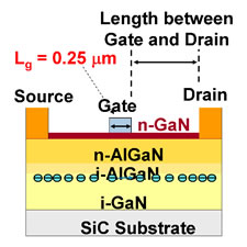 Figure 1: Fujitsu's newly-developed X-band HEMT
Larger View (142 KB)
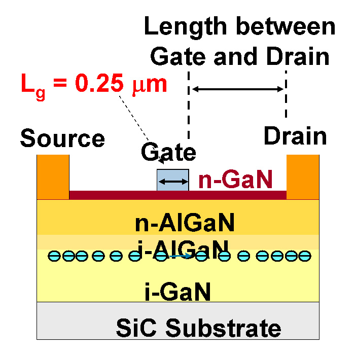
 Figure 2: Circuit structure of Fujitsu's new amplifier
Larger View (99 KB)
Results
The aforementioned technologies were used to develop two types of GaN HEMT amplifiers, for the X band and C band.
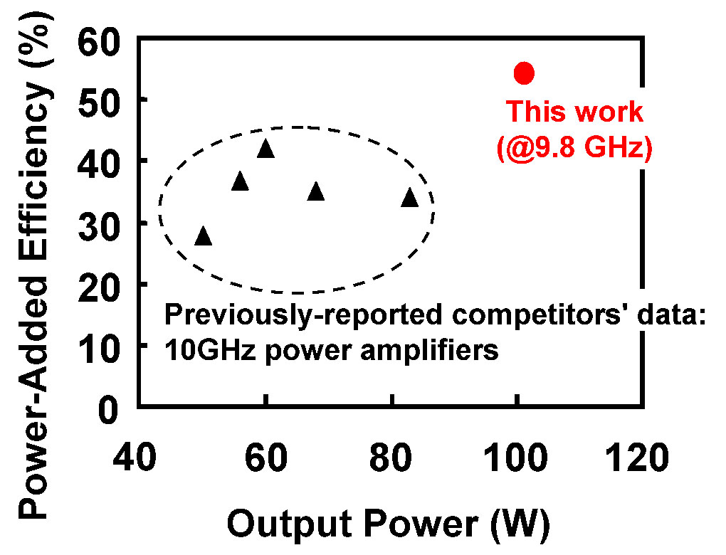
In the X band, this resulted in the world's highest efficiency at 53% and high output of 101 W, as well as good characteristics (Figure 3). Efficiency is especially important for reducing power consumption by the transmitter. Compared to previously-reported results, with equivalent output in the 10 GHz band, efficiency was approximately 20% higher, thus significantly contributing to power savings. Moreover, the 101 W output that was generated was roughly four times greater than output generated with GaAs HEMT amplifiers (according to comparisons made by Fujitsu), allowing for reach to be extended by potentially up to two times.
Additionally, in the C band, this technology maintains levels of efficiency announced by Fujitsu in 2008, while also increasing output which reaches 343 W. This significantly improves upon the figure of 320 W, which was the world's highest when Fujitsu reported it last year. At 343 W, this amplifier outperforms GaAs-based amplifiers by a factor of seven (according to comparisons made by Fujitsu Laboratories), allowing for reach to be extended by potentially a factor of 2.6 times.
The results raise the prospect of using these amplifiers as alternatives to traveling-wave tube amplifiers in high-output applications, which would enable the realization of compact, lightweight, low-power, durable transmission systems in radars, satellite transmitters, and advanced mobile-phone base stations.
Future Developments
Fujitsu plans to apply these technologies to a wide range of applications for which the combination of high- output and high-efficiency performance is demanded, including as alternatives to traveling- wave tube amplifiers used in weather and air-traffic control radars, satellite communications, and next-generation mobile-phone base stations for wireless communications equipment,
 Figure 3. X-band high-output amplifier performance comparison (10 GHz band)
Larger View (135 KB)
-
[1] X band
Name for the frequency band from 8 GHz to 12 GHz. Has less interference and crosstalk, and is not susceptible to jamming. Used in satellite communications, air-traffic control radar, weather radar, etc.
-
[2] Efficiency
With direct DC input power, this expresses the difference between high-frequency output power and high-frequency input power, or the ratio that is converted to amplified output. It is an index expressing the rate at which DC power supplied to an amplifier is converted to high-frequency output in the form of an output signal.
-
[3] Gallium nitride
Used in wide band-gap semiconductors as an alternative to silicon or gallium arsenide. Features high tolerance against breakdown attributable to high voltage.
-
[4] High electron-mobility transistor (HEMT)
A field-effect transistor that takes advantage of operation of the electron layer at the boundary between different semiconductor materials, that is relatively rapid compared to that within conventional semiconductors. This transistor was invented in 1979 by Dr. Takashi Mimura and Fujitsu led the industry with its development of HEMT technology in 1980, and it is currently used in a number of IT applications, including satellite transceivers, cellular equipment, GPS-based navigation systems, and broadband wireless networking systems.
-
[5] C band
Name for the frequency band from 4 GHz to 8 GHz; prone to attenuation by rain and fog. Used in satellite communications, fixed-point wireless access, wireless access, air-traffic control radar, weather radar, etc.
-
[6] Traveling-wave tube amplifiers
A type of vacuum tube used to amplify microwaves. It creates an electron beam that travels at roughly the same speed as the microwave's phase velocity. Speed and density adjustments to that electron beam amplify the microwave, through mutual interaction between the two.
-
[7] Solid-state device amplifier
An amplifier that uses semiconductors made of silicon, gallium arsenide, etc. as active elements.
-
[8] Gain
An index of the ratio between output power and input power (output power divided by input power). Expresses the rate of input-power amplification.
About Fujitsu Laboratories
Founded in 1968 as a wholly owned subsidiary of Fujitsu Limited, Fujitsu Laboratories Limited is one of the premier research centers in the world. With a global network of laboratories in Japan, China, the United States and Europe, the organization conducts a wide range of basic and applied research in the areas of Multimedia, Personal Systems, Networks, Peripherals, Advanced Materials and Electronic Devices. For more information, please see:http://jp.fujitsu.com/group/labs/en/
Technical Contacts
Advanced Devices Lab.Devices & Materials Lab.
![]() Phone: +81(46)250-8229
Phone: +81(46)250-8229
![]() E-mail: gan-hemt-press@ml.labs.fujitsu.com
E-mail: gan-hemt-press@ml.labs.fujitsu.com
Company:Fujitsu Laboratories Ltd.
Company and product names referenced herein are trademarks or registered trademarks of their respective owners. Information provided in this press release is accurate at time of issue and is subject to change without advance notice.
Date: 12 June, 2009
City: Kawasaki, Japan
Company:
Fujitsu Laboratories Ltd.,
,
,
,
,