Tokyo and Kawasaki, Japan, September 19, 2017
Fujitsu Limited, the New Energy and Industrial Technology Development Organization (NEDO), and the Photonics Electronics Technology Research Association (PETRA) today announced development of compact, high-capacity optical transceiver technology that, being compact and high capacity, operates at approximately 400Gbps/cm squared, the world's highest transmission density, roughly double that of previous technology. At the same time, they also developed four-level-pulse control optical modulation transmission technology, which enables 56Gbps per channel high-speed data transmission with a reduction in power consumption of about 40% versus previous technology.
These developed technologies demonstrate promise in contributing to substantial improvements to future server processing speeds.
Details of this technology were announced at the European Conference on Optical Communication 2017, an international conference held in Gothenburg, Sweden on September 17-21.
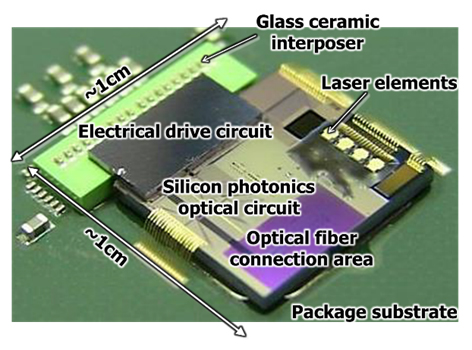
 Figure 1: Newly developed silicon photonics optical transceiver
Summary
To accommodate the digital transformation associated with such technologies as AI and IoT, the scale of systems connecting multiple processors is being increased to improve the performance and efficiency of existing server systems. Accordingly, the expansion of data transmission capacity within server systems has become a major challenge. Because there are limits to data transmission using existing electric circuits, however, there are high expectations for methods that transmit data using light. Specifically, methods which aim to increase capacity for the system as a whole by employing multiple optical elements and multiple electric circuits to drive them are being actively studied (Figure 2). In light of this background, PETRA, Fujitsu Limited and Fujitsu Laboratories Ltd. came together for the "Integrated Photonics-Electronics Convergence System Technology" joint research as part of the NEDO project, developing high density, miniature optical transmitter technology, as well as high speed, low power transmitter technologies, with the goal of expanding data transmission capacity.
Now, Fujitsu, NEDO and PETRA have developed silicon photonics(1) optical transceiver technology with the world's highest density. With a chip size of about 1 cm squared which can be mounted on a processor package, the technology operates at 400Gbps, with 25Gbps across 16 channels (Figure 1). In addition, to accelerate the speed of the new optical transceiver, the organizations have also developed the PAM4(2) optical transmitter technology, which can transmit at the high speed of 56Gbps per channel with a reduced power consumption of 1.6mW per 1Gbps, a reduction of 40% over previous technology.
By installing multiple high-density optical transceivers near a processor, the newly developed technology enables optical transmissions with the bandwidth of about 2Tbps (double the bandwidth of the previous technology). Accordingly, this is expected to significantly improve server processing speeds.
Results
With existing optical transceivers, there were structural limits on the size of the laser elements that could be installed in optical circuits and on the number of channels in the electrical drive circuits, restricting the size and capacity of optical circuits. In addition, because the distance between transmitters and receivers is reduced by increasing the density of optical transmitters and receivers, causing electrical interference in the signal, there were challenges in controlling to minimize this effect when installing transmitters and receivers at high density. Features of the new technology that have overcome these issues are as follows.
1. Compact, high capacity silicon photonics optical transmission technology
(a) Compact, high capacity optical circuit technology
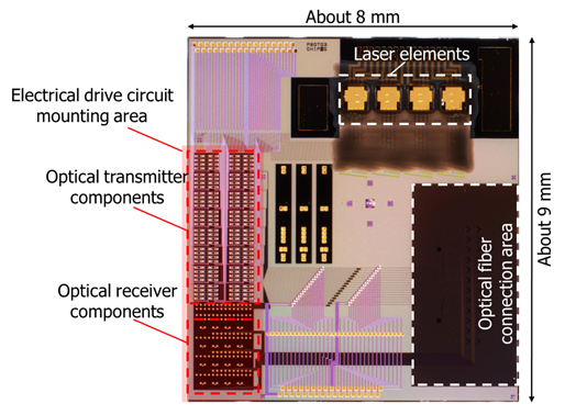
The new miniature silicon photonics optical circuit (8mm x 9mm) can operate at 400Gbps (Figure 3). This optical circuit consists of an optical transmission component with 16 optical modulators(3) and an optical receiver component with 16 photodetectors. PETRA has developed technology for mounting multiple laser elements, which are the light source for optical circuits in silicon photonics, and this technology has now been applied to an optical transceiver for the first time.
It is necessary to incorporate laser elements as a light source for optical circuits. However, it was difficult to simply form them into one circuit, because the structure of the terminal was different from that for connecting the electrical drive circuits. Now, by using a method called "lift-off(4)" to form the laser element mounting terminal, PETRA has established a technique for forming these two types of terminals on silicon photonics, creating a new optical circuit terminal structure for optical transceivers. In addition, the organizations have arranged the structure of the optical circuit in such a way that the laser elements, electrical drive circuits, and the optical fibers connected to the components that handle the input/output of optical signals will not interfere with one another, achieving high capacity in a minimal chip size.
 Figure 3: Newly developed silicon photonics optical circuit
(b) High density electrical interface technology
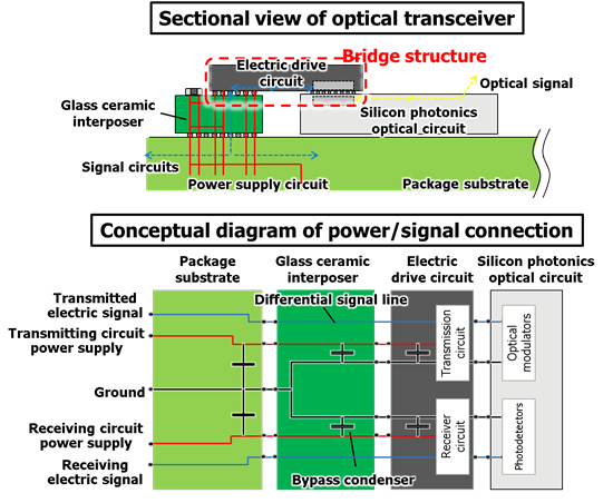
In order to create high density optical transceivers, it is necessary to connect numerous input/output pathways for electrical signals and their power supplies in such a way that they do not interfere with one another. PETRA had previously developed a mounting structure in which a two-dimensional array of high density terminals were connected to the electrical drive circuit through a glass-ceramic interposer that could relay high speed and high density electrical signals, while the electrical drive circuit forms a bridge connecting the glass-ceramic interposer with the silicon photonics optical circuit (Figure 4). This has now been applied to optical transceivers for the first time, enabling the high quality and high density delivery of both the electrical signal and the power supply. The organizations also controlled to minimize the degradation in receiver performance due to electrical interference between the transmitter and receiver components of the optical circuit by implementing a shield structure between them, controlling electrical interference. They also improved power supply quality by reducing noise through the arrangement of the circuitry within the glass-ceramic interposer, utilizing the high circuitry density which is a feature of the bridge mounting structure.
PETRA conducted the overall design and the packaging technology development for this new technology on the basis of circuitry and optical fiber assembling technology developed by Fujitsu Laboratories Ltd.
 Figure 4: Equipped optical transmitter/ Circuit structure
2. High-speed and energy efficiency-enhancing technology
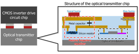
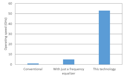
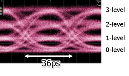
In addition, to further accelerate the newly developed optical transceiver technology, the organizations have simultaneously developed the PAM4 optical transmitter technology, which uses the method of controlling the transceiver with the pulse amplitude modulation of four levels of voltage value to perform transmissions of high-speed optical signals of 56Gbps with a reduced power consumption of 1.6mW per 1Gbps, a reduction of 40% over previous technology (Figures 5). PETRA had been developing optical transmitters with a frequency equalizer made up of passive elements that do not consume power. Now, by directly connecting the electrical circuit driving the optical transmitter to the silicon photonics optical circuit through a solder bump, the circuit's load impedance has been reduced, enabling high speed operation with lower power consumption (Figure 6, 7).
 Figure 5: Structure of the high-speed, energy-efficient optical transmitter
 Figure 6: Comparison of the optical transmitter operating speed
 Figure 7: Waveform of the 56Gbps-PAM4 high speed optical signal
Future Plans
The organizations will apply this new optical transceiver technology to optical modules, with the goal of commercialization by fiscal 2019. By applying its technology to high-density optical transceivers, the NEDO project aims to realize the further development of high-density, energy-efficient optical transceivers.
