Fujitsu

Global

Archived content

NOTE: this is an archived page and the content is likely to be out of date.

Fujitsu Develops GaN Power Amplifier with World's Highest Output Performance for W-Band Wireless Transmissions

Output performance is 1.8 times greater than before, enabling over 30% greater range for high-speed wireless networks

Fujitsu Limited,Fujitsu Laboratories Ltd.

Tokyo and Kawasaki, Japan, January 25, 2016

Fujitsu Limited and Fujitsu Laboratories Ltd. (collectively "Fujitsu") today announced the development of a gallium-nitride (GaN)(1) high-electron mobility transistor (HEMT)(2) power amplifier for use in W-band (75-110 GHz) transmissions. This can be used in a high-capacity wireless network with coverage over a radius of several kilometers.

In areas where fiber-optic cable is difficult to lay, to achieve high-speed wireless communications of several gigabits per second, one promising approach is to use high-frequency bands, such as the W band, which uses a wide frequency band. In order to get good long-distance coverage in these frequencies, however, it is necessary to increase the output power of the power amplifier to the scale of watts.

Fujitsu succeeded in developing a power amplifier for W-band transmissions using GaN-HEMT technology capable of high output at 100 GHz. Evaluations of the newly developed power amplifier confirmed it to have 1.8 times increased output performance than before, which would translate to an increase of over 30% in transmission range when used in a high-speed wireless network.

A portion of this research was conducted as part of a project of the National Institute of Information and Communications Technology (NICT) on "Agile Deployment Capability of Highly Resilient Optical and Radio Seamless Communication Systems."

Details of this technology are being presented at Power Amplifiers for Wireless and Radio Applications (PAWR2016), opening January 24 in Austin, Texas.

Background

High-frequency wireless communications, using the frequency band known as the W band (75-110 GHz), are drawing increasing interest, both as a way to temporarily set up high-capacity communications channels for handling special events where large numbers of people gather, or for responding to disasters, and also as a way to bring communications to remote areas where fiber-optic cables are difficult to lay. Compared to today's mobile phones, which use frequencies in the 0.8-2.0 GHz range, the W band uses a frequency band more than 50 times as broad with 50 times the speed, meaning it is a frequency band that is well-suited to these high-capacity wireless communications.

Issues

In order to transmit wireless signals over a distance of several kilometers, the transmission antenna needs a power amplifier capable of a high output on the order of several watts. Existing power amplifiers for high-frequency transmissions in the millimeter-wave band (30-300 GHz), which are built using gallium arsenide or CMOS semiconductors, are limited by their operating voltage to an output of about 0.1 W, and it has not been possible to increase this.

GaN-HEMT power amplifiers have achieved high output performance in the microwave range (3-30 GHz), but the problem up until now was that their output performance declined in the W-band range.

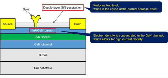
To solve these problems, Fujitsu developed a GaN-HEMT device with a unique structure(3) capable of increasing output in the millimeter band (Figure 1). This uses a layer of indium-aluminum-gallium-nitride (InAlGaN), and double-layer silicon nitride (SiN) passivation film to increase current density by a factor of about 1.4, resulting in 3.0 W of output power from a transistor per 1-mm of gate width, at a high frequency of 100 GHz. In developing this transistor, Fujitsu collaborated with Professor Yasuyuki Miyamoto of the Tokyo Institute of Technology in developing a device-simulation technology.

Figure 1: Cross-sectional diagram of the GaN-HEMT deviceFigure 1: Cross-sectional diagram of the GaN-HEMT device

About the Technology

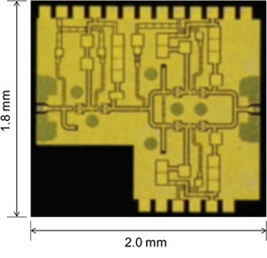
Fujitsu succeeded in developing a power amplifier with the world's highest W-band output performance using this GaN-HEMT device with a proprietary structure (Figure 2).

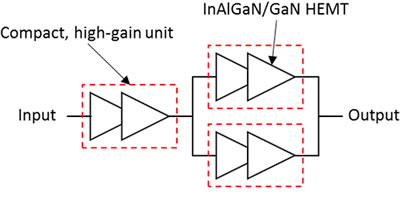
In order to successfully design a power amplifier with high output performance, Fujitsu precisely measured and modeled the characteristics of GaN-HEMT during high-frequency operation. Based on that, a circuit was designed where pairs of GaN-HEMTs were grouped together into compact, high-gain units with low power loss. In order to maximize the power from these units, GaN-HEMTs were connected in a series by the interstage circuit where the signal lines and the device layouts were carefully laid out.

Using a model of these compact, high-gain units, Fujitsu conducted simulations to optimize the distributor and combiner matching circuits between the units, and their layouts and signal lines, resulting in a high-amplitude power amplifier (Figure 3). A prototype power amplifier had amplitude that multiplied its input by a factor of 80, producing 1.15 W of output power. Power output per transistor, a measure of power-amplifier performance, was 3.6 W per 1 mm of gate width, the highest in the world.

Figure 2: Chip containing the newly developed W-band GaN-HEMT power amplifierFigure 2: Chip containing the newly developed W-band GaN-HEMT power amplifier

Figure 3: The compact, high-gain circuit that was usedFigure 3: The compact, high-gain circuit that was used

Results

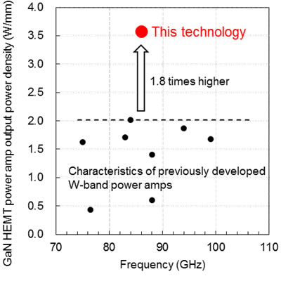
The newly developed power amplifier achieved a 1.8 times increase in power-amplifier output over previous W-band power amplifiers, with the world's highest output performance (Figure 4). This translates to an improvement of over 30% in terms of range for wireless communications at speeds of several gigabits per second.

Figure 4: Performance index of GaN-HEMT power amplifiersFigure 4: Performance index of GaN-HEMT power amplifiers

Future Plans

Fujitsu plans to apply this power-amplifier technology to high-capacity long-range wireless communications, and to implement high-speed wireless communications systems that can be used for high-expediency temporary communications infrastructure for use during special events and when fiber-optic links have been broken in the event of disasters.


  • [1] Gallium nitride

    A wide band-gap semiconductor material that operates with a higher breakdown-voltage than semiconductor technologies based on previous materials, such as silicon (Si)- or gallium-arsenide (GaAs)-based technologies.

  • [2] High electron mobility transistor

    A field-effect transistor that takes advantage of operation of the electron layer at the boundary between semiconductor materials with different bandgaps, which is relatively rapid compared to that within conventional semiconductors. Invented in 1980 by Fujitsu, this technology is currently used in a number of IT applications, including satellite transceivers, cellular equipment, GPS-based navigation systems, and broadband wireless networking systems.

  • [3] GaN-HEMT device with a unique structure

    For details on GaN-HEMT technology, see the presentation announced at the 2015 IEEE International Electron Devices Meeting (IEDM 2015) of December 2015.

About Fujitsu

Fujitsu is the leading Japanese information and communication technology (ICT) company, offering a full range of technology products, solutions, and services. Approximately 159,000 Fujitsu people support customers in more than 100 countries. We use our experience and the power of ICT to shape the future of society with our customers. Fujitsu Limited (TSE: 6702) reported consolidated revenues of 4.8 trillion yen (US$40 billion) for the fiscal year ended March 31, 2015. For more information, please see http://www.fujitsu.com.

About Fujitsu Laboratories

Founded in 1968 as a wholly owned subsidiary of Fujitsu Limited, Fujitsu Laboratories Ltd. is one of the premier research centers in the world. With a global network of laboratories in Japan, China, the United States and Europe, the organization conducts a wide range of basic and applied research in the areas of Next-generation Services, Computer Servers, Networks, Electronic Devices and Advanced Materials. For more information, please see: http://www.fujitsu.com/jp/group/labs/en/.

Press Contacts

Public and Investor Relations Division
Inquiries

Company:Fujitsu Limited

Technical Contacts

Devices & Materials Laboratory


E-mail: E-mail: gan_press_ml@ml.labs.fujitsu.com
Company:Fujitsu Laboratories Ltd.


All company or product names mentioned herein are trademarks or registered trademarks of their respective owners. Information provided in this press release is accurate at time of publication and is subject to change without advance notice.

Date: 25 January, 2016
City: Tokyo and Kawasaki, Japan
Company: Fujitsu Limited / Fujitsu Laboratories Ltd.