![]()
Archived content
NOTE: this is an archived page and the content is likely to be out of date.
Fujitsu Develops World's First On-chip CMOS Power Detector with Temperature Compensation
Requires 1/25th the mounted area, 1/10th the power, contributing to smaller, less expensive smartphones and mobile terminals
Fujitsu Laboratories Ltd.
Fujitsu Laboratories Limited today announced that it has developed a CMOS power detector with built-in temperature compensation, featuring a compact design and low power consumption suitable for use in smartphones and other mobile terminals.
Reducing the mounted area required for components and circuits in mobile terminals is an important factor in reducing their size and cost, but they occupy a relatively large mounted area, because the power detectors used in the transmitters for wireless communications terminals are typically comprised of several radio-frequency (RF) amplifiers. Diodes are known to be an alternative for making power detectors smaller, but their characteristics change with temperature, and the temperature compensation they require has been problematic.
Fujitsu Laboratories has developed a diode-based power detector with a technology that simultaneously enables temperature compensation, resulting in a power detector with a mounted area of only 0.04 mm2 and power consumption of 0.3 mW. Compared to conventional detectors, this requires less than 1/25th the mounted area and consumes 1/10th the power, contributing to smaller, less expensive mobile terminals.
Details of this technology are being presented at ESSCIRC 2012, the European Solid-State Circuits Conference 2012, which opened on September 17th in France.
Background
In recent years, the popularity of mobile terminals such as smartphones and tablets has soared. These mobile terminals are comprised of a large number of internal components; therefore, reducing the mounted area required for these components and circuits is an important factor in reducing overall size and cost.
The transmitters in these mobile terminals require a power amplifier that amplifies and transmits the signal from the mobile terminal to a base station. They also require a power detector that detects the magnitude of that power. Recent mobile terminals have included support for multiple frequency bands, and because a separate power detector is required for the output of each power amplifier for each band, reducing the mounted area for power detectors has become especially important.
Technological Issues
A typical power detector takes a small signal it receives from a power amplifier via a coupler and amplifies it with an RF amplifier, and detection is performed by conversion processing, including rectification (see Figure 1). But amplifying the signal from a power amplifier with wide power-output range requires multi-stage RF amplifiers, which is an obstacle to reducing mounted size.
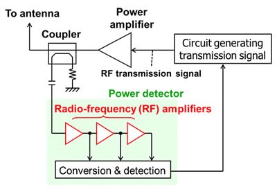 Figure 1: Conventional power detector
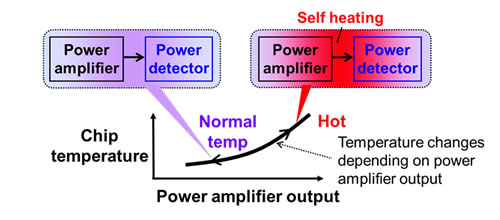 Figure 2: Influence of temperature when power detector is integrated with power amplifier
One method for making smaller power detectors uses diodes for rectification, but integration without temperature compensation will result in power detectors with variable characteristics, because the characteristics of diodes change depending on the temperature. Integrating a diode-based power detector with a power amplifier on one chip will be especially susceptible to the chip's own temperature as the power amplifier heats up. In other words, the temperature that the power detector is exposed to will change (see Figure 2). This self-heating varies in response to the output of the power amplifier, meaning the accuracy of power detection will be degraded by the temperature fluctuations.
About the New Technology
Fujitsu Laboratories has developed a technology that obviates the need for the RF amplifier and applies temperature compensation to diode-based power detection (see Figure 3). Power detection is conducted by generating a current in proportion to the power using a diode.
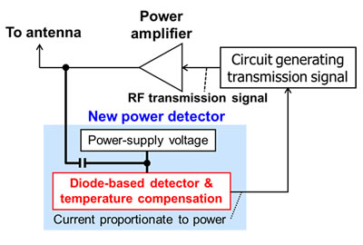 Figure 3: Block diagram of newly developed power detector
To handle temperature fluctuations, a current that varies with the temperature is generated separately using the same diode, and compensation is achieved by subtracting that from the detected current (see Figure 4). Even if the temperature fluctuates, and currents flowing through diodes change, only the current proportionate to the power is detected with no dependency on temperature, because the current equivalent to the temperature fluctuation is being subtracted.
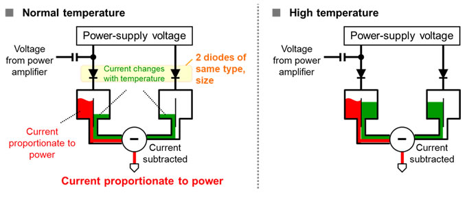 Figure 4: Operation of the newly developed power detector
A power detector based on this technology was fabricated using 90-nm CMOS technology, which resulted in a detector with a mounted area of 0.04 mm2 (compared to roughly 1 mm2 for existing designs) and that operates at 0.3 mW (compared to 5 mW). Accordingly, compared to conventional detectors, the new power detector requires less than 1/25th the mounted area and consumes 1/10th the power.
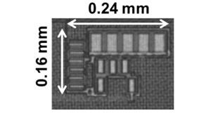 Figure 5: Photograph of the newly developed power detector
Over a range from -30°C to 125°C, this technology achieved detection accuracy on par with conventional detectors (input dynamic range(1) for a detection error within ±0.5 dB is 20 dB or more). This detector supported three frequencies used by WCDMA(2), Band I (2.1 GHz), Band V (850 MHz) and Band IX (1.7 GHz), this circuit technology may be applied to the LTE(3) wireless standard. Owing to its compactness, low-power operation, and temperature compensation, it is amenable to being integrated with power amplifiers.
Results
When combined with commercially available power amplifiers for multiple frequencies, this technology makes possible a dramatic reduction in mounted size for power-amplifier peripherals, contributing to smaller, less expensive mobile terminals.
Future Plans
To apply this technology in practical terms, and make it compatible with future wireless standards, Fujitsu Laboratories plans to continue improving its detection accuracy and expanding its range of power detection.
-
[1] Input dynamic range
Converts an input signal to the equivalent in decibels and expresses the ratio between the maximum and minimum signal levels.
-
[2] WCDMA
Wideband code-division multiple access. A third-generation (3G) mobile communications standard.
-
[3] LTE
Long-term evolution. The latest mobile communications standard in wireless communications terminals.
About Fujitsu
Fujitsu is the leading Japanese information and communication technology (ICT) company offering a full range of technology products, solutions and services. Over 170,000 Fujitsu people support customers in more than 100 countries. We use our experience and the power of ICT to shape the future of society with our customers. Fujitsu Limited (TSE:6702) reported consolidated revenues of 4.5 trillion yen (US$54 billion) for the fiscal year ended March 31, 2012. For more information, please see http://www.fujitsu.com.
About Fujitsu Laboratories
Founded in 1968 as a wholly owned subsidiary of Fujitsu Limited, Fujitsu Laboratories Limited is one of the premier research centers in the world. With a global network of laboratories in Japan, China, the United States and Europe, the organization conducts a wide range of basic and applied research in the areas of Next-generation Services, Computer Servers, Networks, Electronic Devices and Advanced Materials. For more information, please see: http://jp.fujitsu.com/labs/en.
Technical Contacts
Platform Technologies Laboratories
![]() E-mail: powdet@ml.labs.fujitsu.com
E-mail: powdet@ml.labs.fujitsu.com
Company:Fujitsu Laboratories Ltd.
All company or product names mentioned herein are trademarks or registered trademarks of their respective owners. Information provided in this press release is accurate at time of publication and is subject to change without advance notice.
Date: 20 September, 2012
City: Kawasaki, Japan
Company:
Fujitsu Laboratories Ltd.,
,
,
,
,
,
,
,
,
,