![]()
Archived content
NOTE: this is an archived page and the content is likely to be out of date.
Fujitsu Develops World's First Technology to Increase Efficiency of In-Service Optical Network Resources
Enables 40% improvement in transmission capacity, accelerates launch of new optical circuits, and cuts energy consumption by eliminating unnecessary network devices
Fujitsu Laboratories Ltd.,Fujitsu Laboratories of America Inc.,Fujitsu Limited
Fujitsu Laboratories Limited, Fujitsu Laboratories of America, Inc. and Fujitsu Limited today announced the development of the world's first technology for future long-haul and metropolitan optical networks that can dynamically alter the architecture of optical network resources and enhance utilization efficiency without disrupting service.
As a result of the spread of datacenter-centric cloud services, smartphones and other technologies in recent years, a wide variety of network-enabled services are now being offered. At the same time, for the core networks supporting these services, it is important to be able to shorten the time required to bring online new optical circuits that deliver on-demand services, as well as to increase transmission capacity while reducing the energy consumption of network devices. In light of this, Fujitsu has developed two technologies: "flexible optical node" technology that overcomes limitations in terms of optical signal wavelength, modulation scheme and routes; and "spectrum defragmentation(1) technology," which leverages flexible optical nodes to increase the utilization efficiency of in-service optical network resources. This, in turn, makes it possible to improve optical network transmission capacity by up to 40%.
Using the new technology, optical network architecture can be flexibly altered as needed, and given the improvement in the utilization efficiency of network resources, it is possible to accelerate bringing online new optical circuits while reducing power consumption by eliminating unnecessary network devices.
The digital signal processing LSI employed to test the effectiveness of the new technology was developed as part of Japan's Ministry of Internal Affairs and Communications (MIC)'s project for "R&D on Ultra-High-Speed Optical Transmission Technology."
The new technology will be announced at the European Conference on Optical Communications (ECOC) 2012, to be held in Amsterdam from September 16 - 20.
Background
It seems like every day there are ongoing changes in the ways in which networks are employed, including a variety of applications provided through cloud services, which have expanded primarily thanks to large-scale data centers, and high-speed mobile devices as represented by smartphones, as well as sensor networks and other machine-to-machine (M2M) communications. At the same time, for the core networks supporting these applications, optical fiber network technology has begun to enable the implementation of 100 Gbps/channel-class systems, and in the future, transmission systems achieving greater than 400 Gbps are expected to be available. In addition to expanding the capacity of such transmission systems, there is a need to offer end-users a variety of flexible network capabilities without having to increase the power consumed by communications nodes and add excess equipment. Such capabilities include offering high-capacity communications routes for on-demand services, the rapid delivery of alternative routes during major natural disasters, and optimal route selection that enables dynamic route reallocation.
Technological Challenges
The following challenges are evident in bringing about the next generation of high-capacity and flexible optical networks.
1. Limitations to the usable spectrum and communications routes of optical networks
Due to the limitations of optical components and electronic components used inside current optical switch nodes and optical transceivers, it is not possible to freely configure the optical wavelengths, bandwidth, modulation schemes and communications routes employed for communications. As a result, to bring new optical circuits into operation, cables have to be manually rerouted and new equipment deployed.
2. Diminished optical wavelength utilization efficiency as a result of in-service adjustments to communications routes
As a result of constantly adjusting optical spectrum routes while a network is in use, fragmentation can occur in the assignment of optical signals that were initially allocated to optimize network utilization efficiency. This spectrum fragmentation makes it impossible to allocate optical fiber communications routes and bandwidth, a process that is necessary to launch new optical circuits, thereby diminishing the utilization efficiency of transmission equipment.
Newly Developed Technology
To address these challenges, Fujitsu has developed technology that can dynamically adjust the architecture of optical network resources and increase utilization efficiency without disrupting service.
1. Flexible optical node (optical transceivers, optical switches) capable of software-side adjustments to network architecture
Using digital signal processing technology, Fujitsu developed a "universal transceiver" architecture that makes it possible to make software-side adjustments to the transmission schemes of optical transceivers. To accommodate long-haul users, the nodes can be configured to a relatively wide-band transmission scheme employing a highly noise-tolerant modulation scheme that is suitable for long-haul transmissions. For short-haul users, the nodes can be configured to a transmission scheme that is suitable for short-haul transmissions and features high frequency utilization efficiency, but is not very noise tolerant.
With respect to optical switch nodes, communications bandwidth can be adjusted, and through optical switch technology that enables the selection of multiple communications routes, it is possible to perform software-side configuration of communications routes. Combining these routes enables a single optical switch node to be shared among multiple users, flexible configuration to meet users' needs, and realization of flexible optical nodes that can be configured (Figure 1)
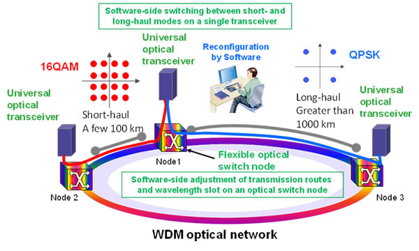 Figure 1: Optical network using flexible optical node technology
2. Improved utilization efficiency of in-service spectrum resources through spectrum defragmentation
Fujitsu has developed a network control mechanism that employs a defragmentation algorithm for securing usable bandwidth allocable for high-volume data by consolidating fragmented spectrum into an uninterrupted spectrum continuum. Using a flexible optical node device architecture, fragmented optical spectrum resources are continuously consolidated into a wavelength band of a size that is allocable for 400 Gbps-class wide-band signal, all while the network remains in service. By channeling the resulting wavelength band into properly configured optical signals, it is possible to improve the utilization efficiency of spectrum resources.
In an experimental network environment featuring four optical switch nodes, Fujitsu demonstrated—for the first time in the world—the use of defragmentation technology employing digital signal processing technology to shift a 100Gbps DP-QPSK optical signal(2) without disrupting service. By taking advantage of the signal bandwidth made available through the defragmentation process, optical network communications capacity can be improved by 40%.
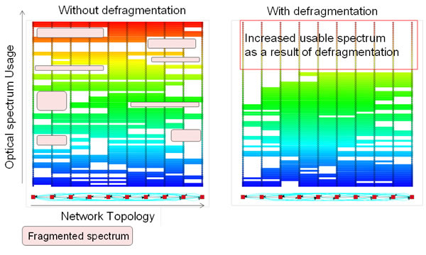 Figure 2: Results of defragmentation
Results
Using the new technology, optical network architecture can be flexibly altered as needed, and given the improvement in the utilization efficiency of network resources, it is possible to shorten the time required to launch new optical circuits, while cutting power consumption by eliminating unnecessary network devices.
Future Development
Fujitsu will work to standardize 400 Gbps-class next-generation interfaces while developing hardware and pursuing R&D on network management systems in aiming to commercialize the new technology.
-
[1] Defragmentation
Just like fragmented storage space on hard disks is consolidated to create larger data space, defragmentation in the case of optical networks is a process of securing usable bandwidth that can be allocated for high-volume data by consolidating fragmented spectrum into an uninterrupted spectrum continuum.
-
[2] DP-QPSK Optical Signal
Dual-Polarization Quadrature Phase Shift Keying. The effective world standard in modulation and demodulation methods for 100 Gbps optical transmission systems.
About Fujitsu
Fujitsu is the leading Japanese information and communication technology (ICT) company offering a full range of technology products, solutions and services. Over 170,000 Fujitsu people support customers in more than 100 countries. We use our experience and the power of ICT to shape the future of society with our customers. Fujitsu Limited (TSE:6702) reported consolidated revenues of 4.5 trillion yen (US$54 billion) for the fiscal year ended March 31, 2012. For more information, please see http://www.fujitsu.com.
About Fujitsu Laboratories
Founded in 1968 as a wholly owned subsidiary of Fujitsu Limited, Fujitsu Laboratories Limited is one of the premier research centers in the world. With a global network of laboratories in Japan, China, the United States and Europe, the organization conducts a wide range of basic and applied research in the areas of Next-generation Services, Computer Servers, Networks, Electronic Devices and Advanced Materials. For more information, please see: http://jp.fujitsu.com/labs/en.
About Fujitsu Laboratories of America
Fujitsu Laboratories of America, Inc. is a wholly owned subsidiary of Fujitsu Laboratories Ltd. (Japan), focusing on research on Internet, interconnect technologies, software development and solutions for several industry verticals. Conducting research in an open environment, it contributes to the global research community and the IT industry. It is headquartered in Sunnyvale, CA. For more information, please see: www.fla.fujitsu.com.
Technical Contacts
Network Systems Laboratories, Photonics Lab
![]() E-mail: fson_pr@ml.labs.fujitsu.com
E-mail: fson_pr@ml.labs.fujitsu.com
Company:Fujitsu Laboratories Ltd.
All company or product names mentioned herein are trademarks or registered trademarks of their respective owners. Information provided in this press release is accurate at time of publication and is subject to change without advance notice.
Date: 19 September, 2012
City: Kawasaki, Japan, Sunnyvale, CA, and Tokyo
Company:
Fujitsu Laboratories Ltd.,
Fujitsu Laboratories of America, Inc.,
Fujitsu Limited,
,
,
,
,
,
,
,