![]()
Archived content
NOTE: this is an archived page and the content is likely to be out of date.
Fujitsu Laboratories Develops Integrated Silicon Optical Transmitter to Carry Large Volumes of Data between CPUs
Demonstrates high-speed operation by integrating light source and optical modulator on the same silicon chip using structure that obviates need for thermal control mechanism
Fujitsu Laboratories Ltd.
Fujitsu Laboratories Limited today announced the development of an integrated silicon optical transmitter for use in an optical transceiver(1), which is essential for enabling large volumes of data to be transmitted between CPUs.
Thermal fluctuations from the heat emitted by CPUs have a large impact on both the light source built into optical transmitters located near CPUs and the optical modulators(2) that encode data into the light emitted from the light source. This means a thermal control mechanism has been required to ensure that the operating wavelengths of both the light source and optical modulator consistently match. Fujitsu Laboratories previously devised a structure incorporating both the light source and optical modulator that did not require thermal control and demonstrated identical thermal properties by using separate prototypes of the light source and the optical modulator. This time, using the same structure to make a prototype optical transmitter that integrates the light source and optical modulator on the same silicon chip, Fujitsu Laboratories demonstrated that it could achieve optical modulation signals at speeds of 10 Gbps at temperatures ranging from 25ºC to 60ºC without a thermal control mechanism. Moreover, the overall electricity consumed by the optical transmitter was reduced by roughly half compared to previous methods.
This technology enables compact, low-power optical transceivers to be mounted directly in CPU packaging. Through its application exaflops-class supercomputers(3) and high-end servers requiring high-speed transmission of large volumes of data, the technology paves the way for super-high-speed computers.
Details of this technology will be presented at the 9th Group IV Photonics international conference (GFP 2012), running August 29-31 in San Diego.
Background
In recent years, supercomputer performance has been roughly doubling every 18 months. Right now, work is underway to produce exaflops-class supercomputers with a target date around 2020. The creation of these ultrafast computers will require high-volume data transmission technology that allows individual CPUs to transfer data to each other at tens of terabits per second. With existing electrical interconnects based on copper wire, however, the dramatic increases required in circuit space, number of transmission lines, and electricity consumption in accordance with the higher data volumes are thought to make it difficult to achieve the data transmission speeds needed for exaflops-class supercomputers. As a result, consideration is being given to the use of optical interconnect technology in which, as shown in figure 1, CPUs are connected using light. Recently, in particular, attention is being focused on the development of silicon photonics(4) technology enabling optical transceivers to be compact and densely integrated, and that enables integration of electrical and optical components.
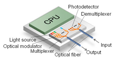 Figure 1. Integrated silicon optical transceiver for large-volume data transmission
Technological Issues
The transmitter component of an optical transceiver comprises a light source and an optical modulator that encodes data into the light emitted by the light source. A good candidate for the optical modulator is a ring resonator(5), as it is compact and energy efficient. But because the optical transceiver is located near the CPU, the lasing wavelength and the operating wavelength of the ring-resonator-based optical modulator do not coincide with each other due to heat from the CPU, resulting in information not being encoded in the light. A thermal control mechanism is needed to ensure that they match exactly, which, however, is an obstacle to making the transceiver compact and energy efficient.
Resolution Approach
By using the same ring resonator for both the wavelength control unit of the light source and the optical modulator, Fujitsu Laboratories previously devised a structure that made the wavelengths of the light source and optical modulator identical without the need for a thermal control mechanism. It used this structure to build separate prototypes of the light source and optical modulator, and it previously demonstrated that their thermal properties were identical.
Newly Developed Technology
This time Fujitsu Laboratories made a prototype optical transmitter that integrates on the same silicon chip a light source and optical modulator employing the previously devised structure. Using this transmitter, it demonstrated that it could make the wavelengths of the light source and optical modulator identical without the need for a thermal control mechanism and could achieve optical modulation signals at speeds of 10 Gbps at temperatures ranging from 25ºC to 60ºC.
Figure 2 depicts the prototype silicon optical transmitter that integrates the light source and optical modulator. To enable shifts in the wavelengths caused by temperature changes to match, the same ring resonator is used for both the wavelength control unit of the light source and the optical modulator. Moreover, to safeguard operation even if there are slight differences in the wavelengths of the light source and optical modulator, the optical modulator is structured with an alignment of multiple ring resonators, increasing the operating wavelength range. Using this structure, there is no need for a thermal control mechanism, and the overall electricity consumed by the optical transmitter was reduced by roughly half compared to previous methods. It is compact, measuring roughly only 2 mm long without the semiconductor optical amplifier. Through optimization using the silicon wire optical waveguide structure(6), it is expected that in the future the size can be reduced to under 1 mm.
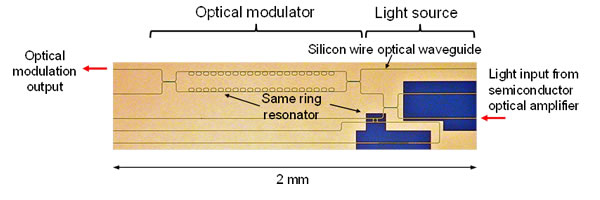 Figure 2. Prototype optical transmitter integrating light source and optical modulator
Figure 3 depicts the optical modulation signals measured at speeds of 10 Gbps at varying temperatures. When varying the temperature from 25ºC to 60ºC, the spectrum's peak wavelength moves to the long-wavelength side, but a stable modulation signal is derived without controlling the wavelengths.
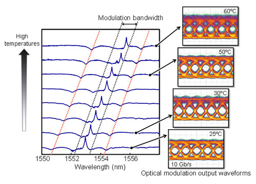 Figure 3. 10 Gbps high-speed modulation operation of the optical modulator at 25ºC - 60ºC
By further increasing the speed of this optical transmitter and integrating multiple transmitters on one chip using wavelength multiplexing technology, it will be possible to create optical transmitters small enough to be embedded into CPU modules capable of transmitting large volumes of data at rates of several terabits per second.
Results
The use of this technology enables the development of exaflops-class supercomputers and high-end servers requiring energy efficient transmission of large volumes of data between CPUs, thereby paving the way for super-high-speed computers.
Future Plans
Fujitsu Laboratories plans to continue development of the optical receiver using the same silicon photonics technology, and will integrate it and this new transmitter to create a compact optical transceiver. Moreover, by applying wavelength multiplexing technology and pursuing dense integration, it will work on developing large-capacity integrated optical interconnects capable of enabling data transmission speeds of tens of terabits per second.
-
[1] Optical transceiver
A module that converts an electrical signal to an optical signal, which it then transmits, and that also receives an optical signal and converts to an electrical signal.
-
[2] Optical modulator
An optical component that converts electrical signals to optical signals. These include intensity modulators that convert to an optical-intensity signal and phase modulators that convert to light-phase signals.
-
[3] Exaflops-class supercomputer
A supercomputer that can process 10 to the18th "FLoating-point number Operations Per Second."
-
[4] Silicon photonics
Technology in which a photonic device is configured on a silicon substrate. By using silicon, the optical circuits can be made smaller, enabling dense integration. It also has other merits, such as the ability to configure optical circuits and electrical circuits in one unit, and lower manufacturing costs.
-
[5] Ring resonator
A resonator made of a ring-type optical waveguide. When used in silicon photonics, this can be made extremely small, with a radius on the order of microns. The ring's resonance effect makes it possible to create a highly efficient optical modulator.
-
[6] Silicon wire optical waveguide structure
An extremely small silicon optical waveguide, in which the height and width of the cross-sectional surface is less than 1µm.
About Fujitsu
Fujitsu is the leading Japanese information and communication technology (ICT) company offering a full range of technology products, solutions and services. Over 170,000 Fujitsu people support customers in more than 100 countries. We use our experience and the power of ICT to shape the future of society with our customers. Fujitsu Limited (TSE:6702) reported consolidated revenues of 4.5 trillion yen (US$54 billion) for the fiscal year ended March 31, 2012. For more information, please see http://www.fujitsu.com.
About Fujitsu Laboratories
Founded in 1968 as a wholly owned subsidiary of Fujitsu Limited, Fujitsu Laboratories Limited is one of the premier research centers in the world. With a global network of laboratories in Japan, China, the United States and Europe, the organization conducts a wide range of basic and applied research in the areas of Next-generation Services, Computer Servers, Networks, Electronic Devices and Advanced Materials. For more information, please see: http://jp.fujitsu.com/labs/en.
Technical Contacts
Next-Generation Manufacturing Technologies Research Center
![]() E-mail: si-photonics-2@ml.labs.fujitsu.com
E-mail: si-photonics-2@ml.labs.fujitsu.com
Company:Fujitsu Laboratories Ltd.
All company or product names mentioned herein are trademarks or registered trademarks of their respective owners. Information provided in this press release is accurate at time of publication and is subject to change without advance notice.
Date: 31 August, 2012
City: Kawasaki, Japan
Company:
Fujitsu Laboratories Ltd.,
,
,
,
,
,
,
,
,
,