![]()
Archived content
NOTE: this is an archived page and the content is likely to be out of date.
Fujitsu Laboratories Develops Technology for Compact Optical Transceivers that Double Data Transmission Speeds to 25 Gbps
Intended for data communications in next-generation servers using optical interconnects
Fujitsu Laboratories Ltd.
Fujitsu Laboratories Limited today announced the development of a compact, cost-effective optical transceiver, a necessary step toward developing optical interconnects for high-speed, high-bandwidth data transmission among CPUs in the next generation of servers.
The data rate and space available for mounting the optical transceivers in use today are obstacles in the way of making future high-performance servers a reality. Fujitsu Laboratories therefore achieved improvements on the driver IC circuit and module packaging structures, enabling transfer speeds of 25 Gbps over each channel in next-generation interconnects, a necessary step toward doubling conventional transmission rates.
This technology enables high-speed, high-bandwidth data communications among CPUs in a server, and between CPUs and peripheral devices. This also marks a significant step toward the improved performance that future supercomputers and high-performance servers will demand.
Details of this technology will be presented at the IEEE 62nd Electronic Components and Technology Conference to be held in San Diego, California on May 29.
Background
Advances in CPU processing power have greatly increased the data-processing capabilities of servers. Now, with improved virtualization technology which allows a single CPU to run multiple processes, the volume of data passing among CPUs and between CPUs and peripherals is vastly increasing. While today's servers use optical interconnects capable of data rates of 10 Gbps per channel, expectations for future servers are that they will be able to run even faster, at 25 Gbps. Furthermore, as Figure 1 illustrates, it is also hoped that optical interconnects can be used not only for data communications among servers, but also among boards within a server, as higher data rates become difficult to achieve with electrical communications.
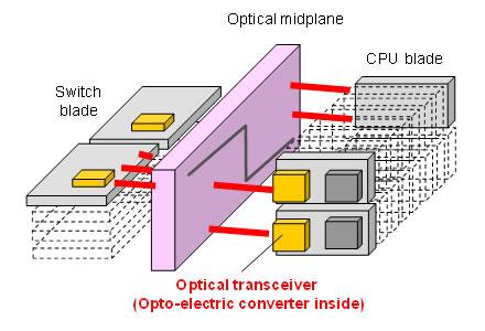 Figure 1: Sample application of optical interconnects in a server
Technological Issues
Implementing optical interconnects within a server requires an optical transceiver that converts electrical signals into optical signals. Current optical transceivers have reached data rates between 10 and 14 Gbps, so the speed of optical transceivers themselves has become a barrier to achieving hoped-for data rates of 25 Gbps. Furthermore, current optical transceivers are physically bulky, making them difficult to place near CPUs or other devices. This is problematic because the electrical signal traveling between the device and optical transceiver encounters line transmission losses and interference that increases with the length of the electrical circuit. This degrades signal quality and makes it more difficult to increase speeds.
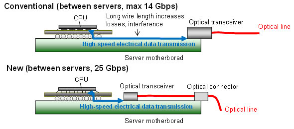 Figure 2: Problems with optical transceivers in optical interconnects used in servers
Newly Developed Transceiver
In order to succeed in producing a compact optical transceiver with the optical interconnects necessary for high-speed, high-bandwidth data transmissions inside servers, Fujitsu Laboratories has developed an opto-electric converter to turn electrical (optical) signals into optical (electrical) signals through an optical device. Details of the technologies follow.
1. High-speed circuitry technology
Fujitsu Laboratories was able to increase speeds through circuit technology in the IC circuit that runs optical devices by making waveforms of optical signals rise and fall more steeply even in inexpensive optical devices with insufficiently fast response times, and by installing circuit technology that suppresses multiple reflections that degrade the electrical signal's waveform. This resulted in an increase in data rates from the current 10–14 Gbps to 25 Gbps per channel.
2. Compact Optical Coupling Technology
Conventionally, efficiently transmitting optical signals between opto-electric converters and optical fiber (optical coupling) required an optical coupling unit that consisted of a lens component and an optical connector (Figure 3). However, the size of the lens component was large and the cost was high. This new construction consists of an opto-electric converter with a flexible printed circuit board that has been equipped with optical devices and ICs, allowing for a compact optical transceiver. In addition, Fujitsu Laboratories has also developed a cost-effective film-type lens sheet which is stacked on the underside of the flexible printed circuit board, thereby solving the problems mentioned above.
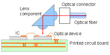 Figure 3: Structure of a conventional opto-electric converter (cross-sectional view)
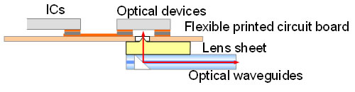 Figure 4: Structure of newly developed opto-electric converter (cross-sectional view)
These technologies were used on a prototype of a 4ch x 25 Gbps opto-electric converter. With a size of 22 mm x 9 mm x 0.86 mm (including on-board electrical components and optical waveguide), the lens component is less than one-tenth as large as conventional lens components in opto-electric converters, while the overall unit has been slimmed down to one-third the conventional size. Taking advantage of its thin size, Fujitsu Laboratories developed optical transceivers with the prototype opto-electric converters placed on the both side. Transmitters and receivers both utilize eight channels with a compact size of 47.8 mm x 16 mm x 21.6 mm, enabling adjacent devices such as the CPU on the printed circuit board to occupy a smaller area.
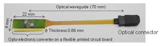 Figure 5: Prototype opto-electric converter
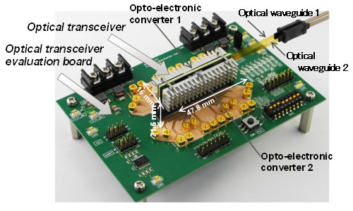 Figure 6: The optical transceiver employing the newly developed technolgy
Results
These technologies achieve 25 Gbps per channel compactly and cost-effectively, the capacity required for next-generation interconnects. This paves the way for high-speed, high-bandwidth communications in servers.
Future Plans
Fujitsu Laboratories is proceeding with research and development to apply this technology to high-performance servers, with the goal of practical use in servers within three years. It also plans to extend this technology more widely to increase the performance of information and communications equipment.
About Fujitsu
Fujitsu is the leading Japanese information and communication technology (ICT) company offering a full range of technology products, solutions and services. Over 170,000 Fujitsu people support customers in more than 100 countries. We use our experience and the power of ICT to shape the future of society with our customers. Fujitsu Limited (TSE:6702) reported consolidated revenues of 4.5 trillion yen (US$54 billion) for the fiscal year ended March 31, 2012. For more information, please see http://www.fujitsu.com.
About Fujitsu Laboratories
Founded in 1968 as a wholly owned subsidiary of Fujitsu Limited, Fujitsu Laboratories Limited is one of the premier research centers in the world. With a global network of laboratories in Japan, China, the United States and Europe, the organization conducts a wide range of basic and applied research in the areas of Next-generation Services, Computer Servers, Networks, Electronic Devices and Advanced Materials. For more information, please see: http://jp.fujitsu.com/labs/en.
Technical Contacts
Network System LaboratoriesPhotonicst Lab.
![]() E-mail: optical-connect-trs@ml.labs.fujitsu.com
E-mail: optical-connect-trs@ml.labs.fujitsu.com
Company:Fujitsu Laboratories Ltd.
All other company or product names mentioned herein are trademarks or registered trademarks of their respective owners. Information provided in this press release is accurate at time of publication and is subject to change without advance notice.
Date: 31 May, 2012
City: Kawasaki, Japan
Company:
Fujitsu Laboratories Ltd.,
,
,
,
,
,
,
,
,
,