![]()
Archived content
NOTE: this is an archived page and the content is likely to be out of date.
Fujitsu Succeeds at Large-Scale Calculations Enabling the Computational Design of Novel Nanodevices
Supercomputer employed to simulate the electrical properties of 1,000-atom models
Fujitsu Laboratories Ltd.
Fujitsu Laboratories Ltd. today announced that it has succeeded at simulating the electrical properties of 1,000-atom models, thereby laying the groundwork for the computational design of novel nanodevices. Since it is possible to treat several times more atoms than in previous undertakings, Fujitsu Laboratories is able to produce results for nanodevices by inputting the model's data into a computer. By eliminating the necessity of repetitive testing as had been required in the past, the new technology is expected to cut costs and accelerate the commercialization of nanodevices.
At the nanoscale, minor differences in the local atomic configuration can have a major impact on the electrical properties of a device. Consequently, it has been impossible to accurately predict the electrical properties of a new structure's configuration using existing data. By employing the "first-principles method"(1) —which can accurately calculate physical properties only from the data of the atomic configuration—to perform highly efficient parallel computations of large-scale calculations, Fujitsu Laboratories was able to simulate the electrical properties of 1,000-atom models, a prerequisite of nanodevice design.
The new technology opens the door to the design of exceptionally high-speed, energy-efficient nanodevices that break totally new ground with their development.
A report on this research will be published on August 11, 2011 in the online edition of Applied Physics Express (APEX).
Background
Transistor channels (electrical conduits) found in today's LSI devices are made from silicon. As devices have become increasingly compact, there has been a heightened level of both operating speed and energy-efficiency. In recent years, however, with the limits of miniaturization continuing to draw near, it has more and more become a challenge to squeeze additional performance from chips. This has led to efforts to develop a completely novel next-generation medium for transistors.
Nanotechnology can be used to create new materials and devices by fabricating substances on the nanometer scale (1.0 × 10⁻⁹ meter). Changes to the atomic geometry, even of the same kind of atoms, can lead to the production of substances with completely different properties. Therefore such technology needs research from the atomic level.
Nanocarbons are one of the better-known examples of a nanomaterial produced through nanotechnology. Nanocarbons include the carbon material graphene, the subject of experiments honored by the 2010 Nobel Prize in Physics, and carbon nanotubes, which were discovered in 1991. These have been recognized for featuring many properties that are ideal for applications in devices, and this has led to high hopes in a wide range of industries for the development of completely novel devices.
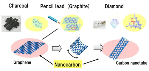 Figure 1: Carbon materials in which changes in atomic geometry completely change the material's properties
Larger View (62 KB)
Technical Issues
During the development of a totally new nanodevice, if the device's electrical properties were accurately calculated using just a computer without testing, it would lead to shortened development times and reduced costs. However, as even minor differences in atomic geometry can significantly impact the electrical properties of a device, until now it has been impossible to predict the electrical properties of a new device using computers.
To accurately predict the properties of a new device, electrical property simulations are performed using first-principles calculations, which precisely calculate from individual atomic data. But given the massive computational requirements of first-principles calculations, the technique's application has been limited to a few hundred atoms. Therefore, until now it has been impossible to perform electric property simulations on the scale of 1,000 atoms, which are thought to be necessary for designing nanodevices.
Newly Developed Technology
Using the OpenMX(2) first-principles calculation program, which has been developed by the Japan Advanced Institute for Science and Technology (JAIST(3)), Fujitsu Laboratories developed a technology that enables the electrical properties of large-scale structures with 1,000 atoms to be definitively calculated.
To compute the electrical properties, calculations are performed repeatedly, each time with a slightly updated input value, until the computations converge. During large-scale first-principles calculations, however, problems arose in which the calculations would simply never finish or they required a considerable amount of time.
In collaboration with JAIST, Fujitsu Laboratories made improvements to the program and its operating methodology to ensure that the first-principles calculations would finish after relatively few iterations.
Although the first-principles calculations require substantial computing time and memory, a large-scale model was successfully calculated using one-third (1,024 cores) of the computing resources of the FX1 supercomputer at the Information Technology Center, Nagoya University(4), along with the deployment of a highly efficient hybrid parallel processing technique(5). By combining the improved first-principles calculation program with a supercomputer, it is possible to calculate the electrical properties of a 1,000 atom-scale model in approximately three days.
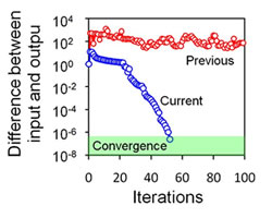 Figure 2: Overview of the technology
Larger View (52 KB)
Results
Graphene and carbon nanotubes feature extremely high electron mobility. With their development, the combination of graphene electrodes and carbon nanotubes has become a leading candidate for new all-carbon devices. Among the models studied using the newly developed technology, only the electrical properties of the model found in Figure 3 possess the ohmic properties(6) desirable for use in devices. It was also discovered that the electrical properties of a model vary significantly depending on the length of the nanotubes and contact structure. These results would have been impossible using conventional empirical methods and first-principles calculations with a limited number of atoms.
In summary, by simulating the electrical properties of models with 1,000 atoms, it was possible to determine the electrical properties of a realistic nanodevice structure, thereby significantly paving the way to designing novel nanodevices.
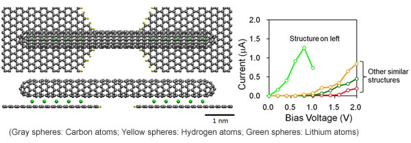 Figure 3: 1,002-atom model (top and side views) and its electrical properties (current/voltage)
Larger View (75 KB)
Future Plans
By developing technology that can efficiently perform larger-scale calculations with computers, Fujitsu Laboratories aims to extend these techniques not only to simulating the electrical properties of nanodevices but to simulations of materials design from the atomic level. Together with the aim of virtual manufacturing using computers, this will contribute to the development of novel nanodevices.
-
[1] First-principles method:
A method of calculating physical characteristics, based on quantum mechanics that electrons and atoms follow, that does not use experimental data or empirical parameters.
-
[2] OpenMX:
Open-source package for Material eXplorer
-
[3] JAIST:
President: Tatsuya Katayama; Location: Nomi City, Ishikawa Prefecture.
-
[4] Information Technology Center, Nagoya University:
Director: Kiyoshi Akusa; Location: Nagoya, Aichi Prefecture.
-
[5] Hybrid parallel computing:
A method of parallel processing that combines both process-parallelization and in-process shared-memory parallelization (multithreading).
-
[6] Ohmic characteristics:
An electric property found in metals in which the electric current is proportionate to the applied voltage.
About Fujitsu Laboratories
Founded in 1968 as a wholly owned subsidiary of Fujitsu Limited, Fujitsu Laboratories Limited is one of the premier research centers in the world. With a global network of laboratories in Japan, China, the United States and Europe, the organization conducts a wide range of basic and applied research in the areas of Next-generation Services, Computer Servers, Networks, Electronic Devices and Advanced Materials. For more information, please see: http://jp.fujitsu.com/labs/en.
Technical Contacts
Next-Generation Manufacturing Technologies Research Center
![]() Phone: +81 (46) 250-8843
Phone: +81 (46) 250-8843
![]() E-mail: simu@ml.labs.fujitsu.com
E-mail: simu@ml.labs.fujitsu.com
Company:Fujitsu Laboratories Ltd.
All other company or product names mentioned herein are trademarks or registered trademarks of their respective owners. Information provided in this press release is accurate at time of publication and is subject to change without advance notice.
This press release has been revised as of December 17, 2018.
Date: 08 August, 2011
City: Kawasaki, Japan
Company:
Fujitsu Laboratories Ltd.,
,
,
,
,
,
,
,
,
,