![]()
Archived content
NOTE: this is an archived page and the content is likely to be out of date.
Fujitsu Shrinks by 70% Distortion-Compensation Circuit for Fiber-Optic Transmissions over 100 Gbps
Expected to enable ultrafast data communications within 5 years
Fujitsu Limited,Fujitsu Laboratories Ltd.,Fujitsu Research and Development Center Co., Ltd.
Fujitsu Limited, Fujitsu Laboratories Limited, and Fujitsu Research and Development Center Co., Ltd. of China today jointly announced that they have developed a digital signal processing algorithm that compensates for waveform distortion in signals sent over hundreds of kilometers of fiber-optic lines, as part of a long-haul transmission system, and that they have also reduced the size of the required circuitry by approximately 70%.
This advance will usher in long-haul fiber-optic transmission systems transmitting data at a rate of more than 100 Gbps per wavelength at a lower cost than conventional 10 Gbps systems in the networks that tie together carrier trunk lines and major datacenters. It had been thought that the practical deployment of such systems would be difficult to achieve even in 10 years, but Fujitsu's new technology is now expected to make it possible within five years.
As a result of these developments, the 10 Gbps lines that predominate in long-haul and regional networks can be replaced with ones that are more than 10 times as fast, ushering in an era of ultrafast communications that have the potential to transform the networked society.
Some of this research was conducted as part of the "Universal Link Project R&D" sponsored by National Institute of Information and Communications Technology (NICT)(1), Japan. Details of this technology are being presented at ECOC2010 (36th European Conference and Exhibition on Optical Communication), opening September 19 in Turin, Italy.
Background
As the volume of data carried over the Internet expands, the fiber-optic lines used to link carrier trunk-line networks and major datacenters are becoming an increasingly important part of network infrastructure, carrying ever-higher levels data. Wavelength division multiplexed (WDM) fiber-optic transmission systems that can carry 100 Gbps per wavelength are expected to go into volume commercial deployment around 2012.
Technological Issues
When transferred over long distances of hundreds of kilometers by fiber-optic lines, ultrafast signals carrying data at speeds of 100 Gbps or more suffer from waveform distortion caused by nonlinear optical effects(2), making it difficult for the signal to be received correctly. This has prompted research into nonlinear compensation technology(3), which can restore the signal received with distortion to a clean waveform. Using conventional methods, however, the implementation of nonlinear compensation technology would require massive circuits with more than 100 million logic gates, and chips that include such compensation circuits are only expected to become feasible around 2020. Reducing the scale required of such circuits, therefore, has been a pressing issue.
About the Newly Developed Technology
Fujitsu's team developed a new signal-processing algorithm, and also was able to dramatically reduce the circuit stages(4) implementing the algorithm to approximately one-quarter of what previously had been required. This was enabled by advances in two areas:
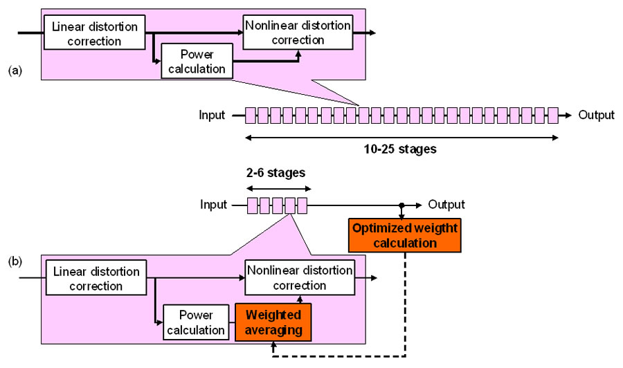
1) Addition of weighted-average processing
In previous technologies, the amount of compensation used to compensate for the distortion in a signal over a given interval was computed based on the signal in only that interval. Fujitsu's new approach is to take into account adjacent intervals, and this approach has been found to allow for fine-grained and accurate compensation using fewer circuit stages. This has been implemented using weighted-average processing.
2) Decision algorithm for weighted-average weighting
In order to compensate the signal accurately and with good granularity using fewer circuit stages, the weight to be given to adjacent intervals can only be decided based on a number of factors, such as transmission distance. The Fujitsu team's development included the ability to automatically determine the ideal weighting at the receiver based on the characteristics of the incoming wave.
Results
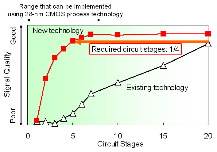
This technology was employed in an experiment to transmit a 112 Gbps signal over 1,200 km. The signal quality using the new five-stage circuit was found to be comparable to that resulting from a conventional 20-stage circuit. By reducing the circuit size, it will be possible to quickly commercialize the technology using 28-nm CMOS process technology, which is expected to be widely used by around 2013. By contrast, using existing technologies, it is anticipated that it would have been challenging to commercialize in less than 10 years.
This technology will allow ultra-high-speed networks using fiber-optic lines to be constructed at lower costs. This would enable, for example, high-definition 3D video to be accessed from anywhere in the world, as well as advanced distance learning and remote medicine technologies.
Future Development Plans
Fujitsu is working to develop next-generation long-distance optical communications systems that operate at speeds of over 100 Gbps and are scheduled for commercialization by 2015. The company is also considering expanding the technology's applications to include high-volume, short-distance transmissions within datacenters and access networks.
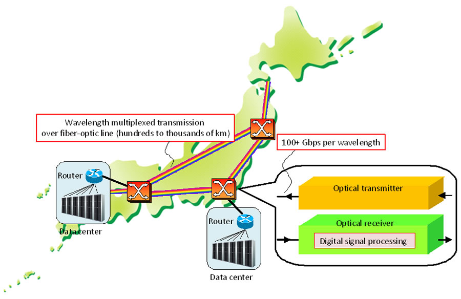
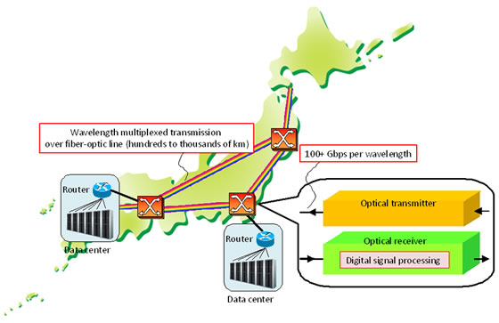 Figure 1. Ultrafast optical transmitters and receivers using digital signal processing in a trunk-line network.
Larger View (75 KB)
 Figure 2. Block diagrams of compensation circuits in existing technology (a) and the new technology (b).
Larger View (59 KB)
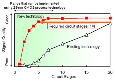 Figure 3: Relationship between signal quality and circuit stages in the existing technology (triangles) and new technology (red squares).
Larger View (52 KB)
-
[1] National Institute of Information and Communications Technology (NICT)
NICT was established in April 2004 as an incorporated administrative agency to carry out research and development in the field of information and communications technology. The agency is based in Tokyo and led by Dr. Hideo Miyahara, president.
-
[2] Nonlinear optical effects
Interactions between light and matter which occur when extremely powerful light passes through fiber optic lines or other materials. The challenge in this instance is a form of what is called self-phase modulation, in which the phase of the light wave changes over an interval in response to its intensity.
-
[3] Nonlinear compensation technology
A technology making it possible to counteract the complex waveform distortion that accumulates from the nonlinear effects occurring at every point on a long-distance fiber-optic line.
-
[4] Circuit stages
In nonlinear compensation technology, because the linear distortion and nonlinear distortion tend to gradually compensate for each other over long-distance transmission lines, the same circuit must be designed so that it has multiple stages of serial connections.
About Fujitsu
Fujitsu is a leading provider of ICT-based business solutions for the global marketplace. With approximately 170,000 employees supporting customers in 70 countries, Fujitsu combines a worldwide corps of systems and services experts with highly reliable computing and communications products and advanced microelectronics to deliver added value to customers. Headquartered in Tokyo, Fujitsu Limited (TSE:6702) reported consolidated revenues of 4.6 trillion yen (US$50 billion) for the fiscal year ended March 31, 2010. For more information, please see: www.fujitsu.com.
About Fujitsu Laboratories
Founded in 1968 as a wholly owned subsidiary of Fujitsu Limited, Fujitsu Laboratories Limited is one of the premier research centers in the world. With a global network of laboratories in Japan, China, the United States and Europe, the organization conducts a wide range of basic and applied research in the areas of Next-generation Services, Computer Servers, Networks, Electronic Devices and Advanced Materials. For more information, please see: http://jp.fujitsu.com/labs/en.
About Fujitsu Research and Development Center
Established in 1998, Fujitsu Research and Development Center Co., Ltd. is a wholly owned R&D center of Fujitsu Limited, located in Beijing. The center's research areas cover the major business fields of the Fujitsu Group, including information processing, telecommunications, semiconductors, and software and services.For more information, please visit: http://cn.fujitsu.com/frdc/.
Technical Contacts
![]() E-mail: nlc@ml.labs.fujitsu.com
E-mail: nlc@ml.labs.fujitsu.com
Company:Fujitsu Laboratories Ltd.
Company, organization, and product names mentioned herein are trademarks or registered trademarks of their respective owners. Information provided in this press release is accurate at time of publication and is subject to change without advance notice.
Date: 21 September, 2010
City: Tokyo and Kawasaki, Japan, and Beijing, China
Company:
Fujitsu Limited,
Fujitsu Laboratories Ltd.,
Fujitsu Research and Development Center Co., Ltd.,
,
,