![]()
Archived content
NOTE: this is an archived page and the content is likely to be out of date.
Fujitsu Develops Technology Enabling Higher-Density Spin-Torque-Transfer MRAM
60% more compact than before; progress toward practical application as a next-generation non-volatile memory
Fujitsu Laboratories Ltd.
Fujitsu Laboratories Limited today announced the development of a new memory cell circuit for spin-torque-transfer MRAM(1) that reverses the typical order of magnetic tunnel junctions (MTJ)(2) to enable a space savings of 60% and achieve a greater degree of integration than was previously possible. Spin-torque-transfer MRAM is regarded as a next-generation non-volatile memory(3) with high potential to become a replacement for NOR-type flash memory.
Currently, microcontrollers for mobile phones and PDAs typically employ NOR-type flash memory, which is approaching its physical limits of miniaturization - however, there is continuous demand for further miniaturization of such non-volatile memory for microcontrollers in handheld electronic devices, as the devices continually become smaller. As a result, spin-torque-transfer MRAM has gained a great deal of attention as a potential successor to NOR-type flash memory, as spin-torque-transfer MRAM can dramatically conserve space, and there has been a significant amount of research aimed at its practical implementation. Fujitsu's new technology paves the way for microcontrollers embedded with spin- torque-transfer MRAM that are more compact, and which can run applications more quickly than microcontrollers embedded with NOR-type flash memory.
Details of the novel technology will be presented at the 2010 Symposium on VLSI Technology (2010 VLSI), held in Honolulu, U.S. from June 15-17 (Presentation number: 5.2).
Background
Many electronic devices, including mobile phones and PDAs, use microcontrollers with embedded flash memory to store software and other data that can be re-written. However, NOR-type flash memory that is used in microcontrollers is expected in the near future to reach the physical limits of its miniaturization, which has prompted research into a number of potential next-generation successor technologies.
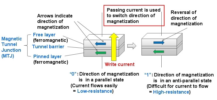
One of these next-generation memory technologies that has attracted a great deal of attention, spin-torque-transfer MRAM, is a memory storage element that makes use of the phenomenon in which passing a current through a magnetic material causes its direction of magnetization to reverse. Passing a current through the material causes the direction of magnetization to either be in a parallel or anti-parallel state. This high or low electrical resistance can be handled in terms of binary digital information, either 1 or 0, enabling the storage element to be used as non-volatile magnetic memory (Figure 1).
Spin-torque-transfer MRAM is expected to become a successor to flash memory not only because of its compact size, but also because of its potential for low power consumption and high performance. This has spurred R&D aimed at practical implementation of spin-torque-transfer MRAM.
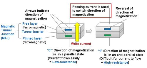 Figure 1: Principles of spin-torque-transfer MRAM
Larger View (51 KB)
Technological Challenges
While it has been possible to miniaturize MTJ elements used in spin-torque-transfer MRAM, shrinking the adjoining cell-select transistors had thus far posed a challenge.
The memory cell circuit in spin-torque-transfer MRAM is a circuit that connects the MTJ element with a cell-select transistor, which act as switches that select which MTJ elements to write to or read from. With existing memory cell circuits, when the MTJ element of a spin-torque-transfer MRAM has been written to a high-resistance state ("1"), voltage is lowered through variable resistance - this requires a larger current to write than when an MTJ element it is switched to a low resistance state ("0"), which is not affected by variable resistance. In other words, because the cell-select transistor's current-driving capability is low, writing to a high-resistance state ("1") would require a significant current. As such, even with a low driving-current capability, cell-select transistors need to be relatively large to ensure an adequate write current, which has been a barrier to reducing transistor size.
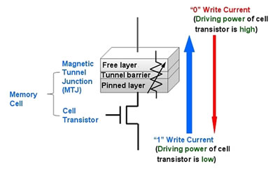 Figure 2: Conventional memory cell circuit
Larger View (30 KB)
Newly-Developed Technology
Fujitsu Laboratories has reversed the order of the MTJ element's magnetic layers, enabling the development of a new MTJ element with a top-pinned structure - that differs from previous structures - that consists of a pinned layer, tunnel barrier, and free layer. However, because the distance between the tunnel barrier of the top-pinned MTJ element and its bottom electrode has been reduced, electrical short failures are more likely to occur during fabrication - as a countermeasure to address this issue, Fujitsu Laboratories has inserted a buffer layer to maintain separation between the tunnel barrier and bottom electrode, which allows the output from the low-resistance ("0") writing to travel in the same direction as the cell-select transistor's low driving-current capacity, thus making it possible for the cell-select transistor to still function at a smaller size.
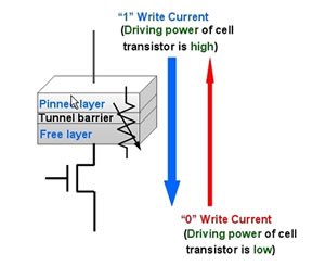 Figure 3: Top-pin memory cell circuit
Larger View (23 KB)
Results
This technology was used to reduce the area of memory cell circuits by 60%, thus enabling a higher degree of integration unattainable with previous spin-torque-transfer MRAMs, resolving one of the technology's key technical implementation challenges for practical use.
Future Developments
Fujitsu Laboratories will continue to develop process technologies for further miniaturization of spin-torque-transfer MRAM components, and pursue other R&D aimed at practical implementation of spin-torque-transfer MRAM.
-
[1] Spin-Torque-Transfer MRAM
Spin Torque Transfer Magnetoresistive Random Access Memory. This is MRAM that uses the "spin-torque-transfer" effect to reverse the magnetic polarity of a magnetic material, by passing a current through it.
-
[2] Magnetic tunnel junction (MTJ)
A tunnel junction that has the magnetoresistive effect. It consists of a recording layer made of strong magnetic material, an insulating film that is a few atoms thick, and a layer made of strong magnetic material that will not change its magnetic orientation in the presence of a current.
-
[3] Non-volatile memory
Memory that persists in the absence of electrical power.
About Fujitsu Laboratories
Founded in 1968 as a wholly owned subsidiary of Fujitsu Limited, Fujitsu Laboratories Limited is one of the premier research centers in the world. With a global network of laboratories in Japan, China, the United States and Europe, the organization conducts a wide range of basic and applied research in the areas of Next-generation Services, Computer Servers, Networks, Electronic Devices and Advanced Materials. For more information, please see: http://jp.fujitsu.com/labs/en.
Technical Contacts
Nanoelectronics Research Center
![]() Phone: +81(46)250-8379
Phone: +81(46)250-8379
![]() E-mail: nanoele-sttmram@ml.labs.fujitsu.com
E-mail: nanoele-sttmram@ml.labs.fujitsu.com
Company:Fujitsu Laboratories Ltd.
Company and product names mentioned herein are trademarks or registered trademarks of their respective owners. Information provided in this press release is accurate at time of publication and is subject to change without advance notice.
Date: 17 June, 2010
City: Kawasaki, Japan
Company:
Fujitsu Laboratories Ltd.,
,
,
,
,