![]()
Archived content
NOTE: this is an archived page and the content is likely to be out of date.
Fujitsu Develops Gallium-Nitride HEMT Amplifier Featuring World's Highest Output in the C-Ku Band
Realizes smaller, lighter radar and communications equipment
Fujitsu Laboratories Ltd.
Fujitsu Laboratories Ltd. today announced the development of an amplifier based on gallium-nitride (GaN)(1)high electron mobility transistor (HEMT)(2) technology, which features an output of 12.9W - more than twice the output of previous amplifiers and presently featuring the world's highest amplification output - when operating in the wide band range of the C-band, X-band, and Ku-band(3) radio frequency spectrums between 6GHz-18GHz. By employing this amplifier, it will be possible to operate systems such as aviation radar - which conventionally utilize separate communications equipment for different frequency ranges - with a single amplifier, thereby enabling the development of smaller, lighter radar equipment and wireless communications systems that are capable of covering wide areas.
Details of this technology will be presented at the IEEE MTT International Microwave Symposium (IMS 2010) being held in Anaheim, U.S. from May 23-28.
About Gallium-Nitride High Electron Mobility Transistors
Gallium-nitride (GaN) is used in blue-LEDs for traffic signal lights, and as a semiconductor material GaN enables electrons to move faster than in conventional semiconductor materials, such as silicon (Si) and gallium-arsenide (GaAs). GaN also features a higher breakdown voltage (threshold) compared to such conventional semiconductor materials.
Given these characteristics, GaN HEMTs - a kind of GaN-based transistor - are anticipated to offer high-output high-efficiency operation.
Background
Aircraft radar typically switches between the C-band, which is relatively unaffected by rain, and the X- and Ku-bands which offer high-precision detection of solid objects. An amplifier featuring the ability to cover - on its own - the entire range of the C- to Ku-bands would allow for smaller systems that consume less power. This has led to keen interest in multifunctional radars, which integrate communications systems and multiple radars and into a single device.
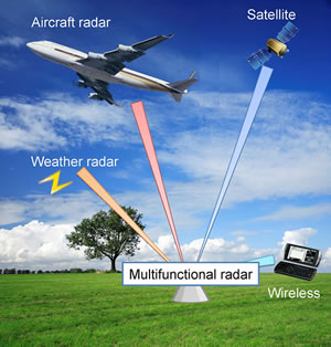 Conceptual image of C-Ku band multi-functional radar
Larger View (148 KB)
Technological Issues
To achieve the output needed to cover large spectrums such as the C- to Ku-bands, in the past multiple transistors have been connected in parallel to create an amplification circuit. However, as the circuit is physically longer, line loss increases, thus making it difficult to extend coverage up to 18GHz.
Newly-developed Technology
Fujitsu Laboratories developed a high-output GaN HEMT amplifier that covers the ultra-broadband C-Ku spectrum (6GHz-18GHz).
Key features of the new technology are as follows:
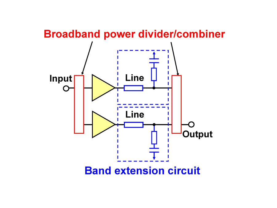
- Band-extending circuit technology:
Fujitsu Laboratories devised a band extension circuit that compensates line losses at high frequencies, and employed the circuit in an amplifier for the first time ever (Figure 1). - Circuit technology for dividing and combining electrical power over broadband:
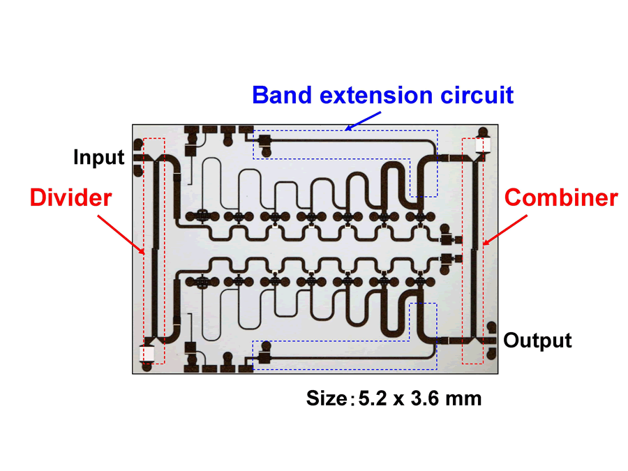
Fujitsu Laboratories developed a circuit that handles the dividing and combining of electrical power across an ultra-wide spectrum, and built the circuit on the semiconductor chip (Figure 2).
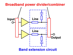 Figure 1: Circuit block diagram Figure 1: Circuit block diagram
Larger View (31 KB) |
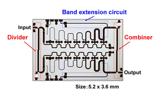 Figure 2: Fujitsu's newly-developed C-Ku band amplifier Figure 2: Fujitsu's newly-developed C-Ku band amplifier
Larger View (98 KB) |
Results
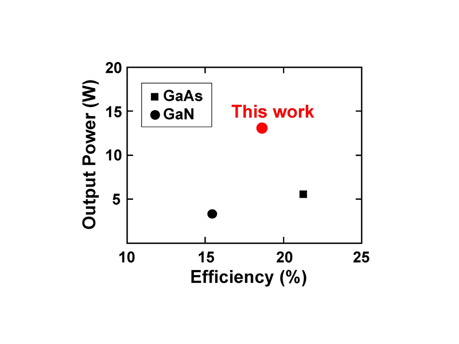
The newly-developed GaN HEMT amplifier was proven to produce 12.9W of power over the wide 6GHz-18GHz spectrum with 18% efficiency(4). This amplification output is more than double (2x) the output of existing ultra-broadband, high-frequency amplifiers, and represents the world's highest level of performance (Figure 3).
This new technology will make it possible for a single amplifier to operate at multiple frequencies, paving the way for further integration of systems, such as broadband communications systems and radar systems that utilize various frequencies, thus allowing for more compact and lighter equipment. The technology can also be used in measuring instruments in order to measure the performance of amplifiers used in broadband communications and radar systems.
 Figure 3: Comparison of C-Ku ultra-broadband amplifier performance
Larger View (17 KB)
Future Developments
Fujitsu Laboratories plans to apply this technology to a wide range of applications that require high output across wide bandwidths, including wireless communications and radar.
-
[1] Gallium-nitride (GaN):
GaN-based semiconductors are wide bandgap semiconductors that feature a higher breakdown-voltage (threshold) than conventional semiconductor materials, such as silicon (Si) or gallium-arsenide (GaAs).
-
[2] High-electron mobility transistor (HEMT):
A field-effect transistor that utilizes the electron movement at the junction between two semiconductors with different band gaps - the electronic movement in HEMTs is faster compared to that of conventional semiconductors. Fujitsu led the industry with its development of HEMT technology in 1980, and HEMTs are currently used in a wide range of core technologies for IT applications, including satellite transceivers, mobile phones, GPS-based navigations systems, and broadband wireless networking systems.
-
[3] C-band, X-band, Ku-band:
Common names for each frequency band. The C-band covers 4GHz-8GHz and is not prone to attenuation from rain or fog. Applications employing C-band include satellite communications, fixed wireless networking, wireless access networking, air-traffic control radar, weather radar, etc. The X-band covers 8GHz -12GHz, and has only minimal impact from crosstalk and interference, thereby making the X-band difficult to be intercepted or jammed. The X-band is often used in satellite communications, air-traffic control radar, and weather radar. The Ku-band covers 12GHz-18GHz, and has only minimal impact from crosstalk and interference, thus making the Ku-band difficult to be intercepted or jammed. Ku-band applications include satellite communications and various types of radar.
-
[4] 18% efficiency:
Efficiency refers to the ratio of the high-frequency (h.f.) output power to the DC input power, taking into account the power amplifier gain.It is calculated as: Efficiency = 100*(h.f. output power – h.f. input power/(DC input power)
About Fujitsu Laboratories
Founded in 1968 as a wholly owned subsidiary of Fujitsu Limited, Fujitsu Laboratories Limited is one of the premier research centers in the world. With a global network of laboratories in Japan, China, the United States and Europe, the organization conducts a wide range of basic and applied research in the areas of Next-generation Services, Computer Servers, Networks, Electronic Devices and Advanced Materials. For more information, please see: http://jp.fujitsu.com/labs/en.
Technical Contacts
Advanced Devices Research Lab.Platform Technologies Lab.
![]() Phone: +81(46)250-8229
Phone: +81(46)250-8229
![]() E-mail: gan-hemt-press@ml.labs.fujitsu.com
E-mail: gan-hemt-press@ml.labs.fujitsu.com
Company:Fujitsu Laboratories Ltd.
Company and product names mentioned herein are trademarks or registered trademarks of their respective owners. Information provided in this press release is accurate at time of publication and is subject to change without advance notice.
Date: 27 May, 2010
City: Kawasaki, Japan
Company:
Fujitsu Laboratories Ltd.,
,
,
,
,