![]()
Archived content
NOTE: this is an archived page and the content is likely to be out of date.
Fujitsu Develops A/D Converter with World's Highest Power Efficiency in Its Class
Compact, with 1/10th power consumption of previous models; lowers environmental impact of digital equipment
Fujitsu Laboratories Ltd.
Fujitsu Laboratories Ltd. today announced the development of a successive-approximation-register (SAR)(1)analog-to-digital converter (A/D converter)(2) that detects variations in electronic characteristics and automatically compensates for them, achieving performance on par with existing pipelined(3) A/D converters, while reducing both the size and power consumption to one-tenth (1/10) that of previously-developed A/D converters. A/D converters often account for a large share of the total power consumed by digital equipment, and previous efforts to reduce their power demands had been challenging. Fujitsu's new technology will pave the way for system LSI devices for mobile phones and digital devices that will be smaller and more power-efficient, thus contributing to reducing the environmental burden attributable to such devices.
Details of this technology were presented at the IEEE International Solid-State Circuits Conference 2010 (ISSCC 2010) being held in San Francisco from February 7-11. (Presentation number: 21.4)
Background
As mobile phones and digital devices have become higher-performance and continuously feature higher functionality in recent years, there has been demand for A/D converters that are concurrently compact and more power-efficient. In digital equipment, the A/D converter often accounts for a large share of the equipment's total power consumption, making it an obvious target for technologies that can reduce power consumption.
Most A/D converters used in digital devices and mobile phones today are pipelined A/D converters used to amplify signals. Since SAR A/D converters - used mostly in control sensors - do not use amplifiers, they are compact and consume less power, making SAR A/D converters attractive candidates as a substitute for pipelined A/D converters.
Technological Challenges
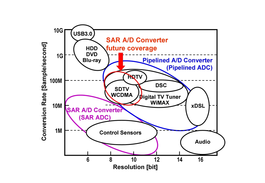
Pipelined A/D converters that are typically used in digital equipment include analog circuitry, which makes further miniaturization of the internal circuitry difficult, and which would require an alternative in order to take advantage of future miniaturization processes. In contrast, SAR A/D converters require only simple internal analog circuits that do not require complex circuitry and have the advantages of small size, good power efficiency, and amenability to miniaturization processes. A shortcoming of SAR A/D converters is that they are not amenable to running at high speeds, since they are susceptible to variations in electronic characteristics that emerge in manufacturing. For this reason, SAR A/D converters have only been used at comparatively low speed ranges of 10 megasamples-per-second (MS/s) or less (Figure 1). A SAR A/D converter that runs fast and makes allowances for variations in electronic characteristics would achieve desirable low power requirements and compact size, and in addition be amenable to future miniaturization processes.
 Figure 1. Overview of various A/D converters and products with on-board A/D converters
Larger View (61 KB)
Newly-developed Technology
Fujitsu Laboratories developed a "digital assist" technology that internally detects and automatically compensates for malfunctions caused by variations in electronic characteristics, as well as variations in temperature and supplied voltage. This removes the design restriction that had previously mandated elements above a certain size, in order to ensure a reliable degree of precision. SAR A/D converters built with this technology can cut power requirements by some 90%, with only one-tenth (1/10th) the surface area for the A/D converter itself.
Results
Fujitsu Laboratories developed a SAR A/D converter with 10-bit resolution and a 50 megasamples-per-second (MS/s) conversion rate. This attained the lowest power consumption(4) (highest power efficiency) of any A/D converter in this class of 820 µW.
Smaller, more efficient A/D converters have ramifications beyond the performance of the A/D converter itself. The system LSI device that the A/D converter is a part of can also be made smaller and more power-efficient, having a significant effect on the power efficiency of the device overall.
Future Developments
Fujitsu Laboratories will proceed to further develop this technology for application in digital home appliances, mobile phones, and in Japan "1seg and Full-Seg" mobile phone digital TV broadcast tuners. Fujitsu will also work on adapting the technology to further miniaturization processes, and plans to use the technology in various other analog circuits as well.
-
[1] Successive-approximation-register (SAR)
A type of analog-to-digital converter in which a single comparator successively makes large or small comparisons. Although the circuit design is simple because it does not require an amplifier, successive-approximation-register A/D converters are not amenable to high-speed operation.
-
[2] Analog/digital converter (A/D converter)
A circuit that converts an analog signal to a digital signal.
-
[3] Pipelined
A type of analog/digital (A/D) converter in which a series of low-resolution conversion circuits, arranged in a pipeline, each determine a separate digit.
-
[4] Lowest power consumption
Specifications are as follows:Resolution: 10 bitsConversion rate: 50 MS/sProcess technology: 65-nm CMOSVoltage: 1.0 VPower consumption: 0.82 mWA/D converter surface area: 0.04 mm2
About Fujitsu Laboratories
Founded in 1968 as a wholly owned subsidiary of Fujitsu Limited, Fujitsu Laboratories Limited is one of the premier research centers in the world. With a global network of laboratories in Japan, China, the United States and Europe, the organization conducts a wide range of basic and applied research in the areas of Multimedia, Personal Systems, Networks, Peripherals, Advanced Materials and Electronic Devices. For more information, please see:http://jp.fujitsu.com/group/labs/en/
Technical Contacts
Design Solutions Lab.Platform Technologies Lab.
![]() Phone: +81(44)754-2690
Phone: +81(44)754-2690
![]() E-mail: saradc@ml.labs.fujitsu.com
E-mail: saradc@ml.labs.fujitsu.com
Company:Fujitsu Laboratories Ltd.
Company and product names mentioned herein are trademarks or registered trademarks of their respective owners. Information provided in this press release is accurate at time of publication and is subject to change without advance notice.
Date: 12 February, 2010
City: Kawasaki, Japan
Company:
Fujitsu Laboratories Ltd.,
,
,
,
,