![]()
Archived content
NOTE: this is an archived page and the content is likely to be out of date.
Fujitsu Develops World's First Millimeter-Wave Gallium-Nitride Transceiver Amplifier Chipset
- Enables higher-performance high-capacity wireless transmission equipment; bridges the digital divide -
Fujitsu Limited,Fujitsu Laboratories Ltd.
Fujitsu Limited and Fujitsu Laboratories Ltd. announced today the development of the world's first gallium-nitride(1)HEMT(2)-based transceiver amplifier chipset for broadband wireless transmission equipment operating in the millimeter bandwidth, the range of 70 to 100 GHz, for which widespread usage is expected to grow. The new transceiver amplifier chipset features a GaN HEMT-based high-output transmitter amplifier and high-sensitivity receiver amplifier. The transmitter amplifier achieves the world's highest level of performance with output of 350 mW, while the receiver amplifier features the world's highest level of signal gain at 310 times (310x) operating in the W-band(3) with a low noise figure(4) of 3.8 decibels (dB). Compared to gallium-arsenide (GaAs)-based technology, the new GaN HEMT-based amplifier chipset for the millimeter band is anticipated to offer output that is increased by approximately four-fold (4x), and a noise figure decreased by 40%, while transmission ranges are expected to be extended by roughly three-fold (3x). Used as an alternative to fiber-optic cabling, Fujitsu's new GaN HEMT-based millimeter-band transceiver amplifier will help bridge the digital divide(5) for wireless communications, by making communications equipment for trunk lines and ultra-high-speed fixed wireless access higher in quality and more compact, ultimately making wireless broadband more practical.
Details of this technology were presented at the European Microwave Integrated Circuits Conference (EuMIC), being held from September 28 to 29 in Rome. Part of this research was conducted as part of the Research and Development Project for Expansion of Radio Spectrum Resources sponsored by Japan's Ministry of Internal Affairs and Communications.
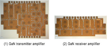 Figure 1: Newly-developed chipset featuring GaN-based high-output transmitter amplifier and high-sensitivity receiver amplifier
Larger View (100 KB)
Background
In order to accommodate the demands for greater bandwidth on the Internet, mobile phone networks, and other networks, fiber-optic cabling is being laid throughout Japan to create a high-capacity trunk-line system. This is problematic in heavily built-up areas, or areas with difficult topography, which has sparked interest in high-bandwidth wireless that is capable of data transmission capacities and speeds of 10 Gbps - on par with fiber-optic cabling - as a way to bridge the digital divide.
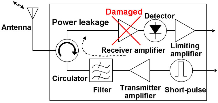
The millimeter-wave band from 70 to 100 GHz would be an effective band to use for wireless communications running faster than 10 Gbps, as it is readily available and is appropriate for long-distances transmissions. Fujitsu and Fujitsu Laboratories have successfully tested millimeter-band transmitters and receivers at speeds of 10 Gbps using impulse radio(6) . In order for this to be practical and widely used, transmission distances would need to be extended from several kilometers to several tens of kilometers. One way to achieve that would be through higher-output amplifiers. However, higher outputs bring with them increased power-leakage from the transmitter to the receiver, which can overload the inputs of circuits using existing indium-phosphide (InP)- and GaAs-based technologies, resulting in breakdowns (Figure 2). As a result, there has been a desire to develop GaN-based receiver amplifiers, as they can tolerate higher inputs and have excellent reception sensitivity.
 Figure 2: Structure of impulse radio millimeter-wave transceiver
Larger View (66 KB)
Technological Challenges
In order to enable a transceiver amplifier that satisfies the aforementioned requirements for W-band signals, the following issues need to be addressed:
1. Compared to conventional GaAs HEMT devices, material used in GaN HEMT devices have wide band-gap characteristics that enable breakdown-voltages that are ten times greater (10x), allowing GaN HEMT devices to tolerate higher voltages. However, because the parasitic capacitance of transistors worsens with high-frequency signals of 70 GHz or higher, the signal amplification rate to magnify weak incoming signals - to enable them to be identified - is insufficient, as the incoming signals become buried in noise.
2. At frequencies above 70 GHz, the signal wavelength is roughly the same length as the chip size, which produces signal interference that is more prominent, between signal paths and circuits. This makes it difficult to create an integrated circuit featuring good signal amplification and low noise, due to the fact that oscillation of the circuit itself can result in malfunctions caused by unnecessary power-coupling between the signal paths.
Newly-Developed Technology
Fujitsu has addressed the aforementioned issues through the following technologies:
1. Technology for GaN HEMT-based circuits featuring high breakdown-voltage and adapted for millimeter wave
In 2006, Fujitsu and Fujitsu Laboratories developed a GaN HEMT structure with gates of only 0.12 µm in length, allowing for both high breakdown-voltage and good high-frequency performance. By tuning this gate structure and adjusting the thickness of the protective layer, parasitic capacitance was reduced, and the increased signal gain further improved noise characteristics (Figure 3).
2. Millimeter-wave circuit stabilization technology
Compared to existing devices, as the output of GaN HEMTs is higher, signal interference - caused by unnecessary signal emissions from signal circuitry - between signal paths and circuits is more prominent in GaN HEMTs. With the newly-developed device, by laying contact conductors around the signal circuitry, while employing a 3-D electromagnetic field analysis to optimize the placement of via-holes that penetrate the top and bottom of the chip relative to signal paths and circuits, and in addition by developing a design technology that shields against unnecessary signal radiation , and applying all of these for the first time ever in GaN HEMT circuitry, signal interference was successfully suppressed. These technologies realize a circuit that features high output and high signal-gain while being able to operate stably, free from malfunctions caused by circuit oscillations (Figure 4).
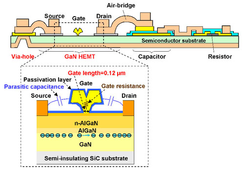 Figure 3: Cross-section diagram of newly-developed high breakdown-voltage millimeter-wave GaN HEMT integrated circuit
Larger View (134 KB)
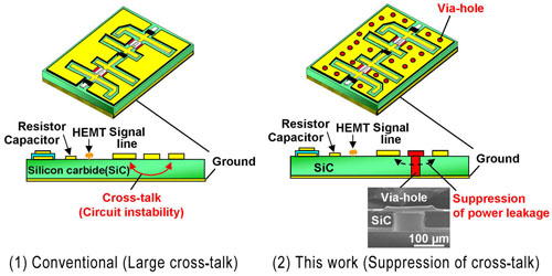 Figure 4: Newly-developed stabilization technology for millimeter-wave circuits
Larger View (139 KB)
Results
The aforementioned technologies have been used to develop a transceiver amplifier chipset for use in millimeter-wave wireless equipment (Figure 1). The newly-developed receiver-amplifier operates in the W-band with a signal gain rate of 25 dB (signal gain is 310x) and a noise figure of 3.8 dB, both figures being the world's best-ever reported for a GaN-based integrated circuit (Figure 5). The amplifier unit's reception performance is on par with those using GaAs-based technology, but because it obviates the need for a protective circuit, the performance of the transceiver as a whole can be expected to improve (Figure 6). In addition, the transmitting amplifier has world-class performance, featuring transmission output of 350 mW.
Compared to GaAs-based technology, the new technology produces output that is roughly four times greater (4x) and reduces the noise figure by 40%. Compared to transceivers based on conventional GaAs technology, transmission ranges can be expected to be three times as great (3x). This will pave the way for wireless transmission equipment that is more compact and which features improved transmission quality.
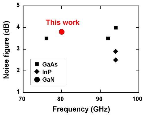 Figure 5: Comparison of millimeter-wave receiver amplifier performance(world's first report for GaN-based)
Larger View (73 KB)
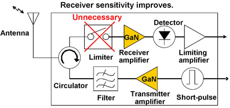 Figure 6: Structure of impulse radio high-performance millimeter-wave transceiver
Larger View (78 KB)
Future Developments
Fujitsu and Fujitsu Laboratories plan to continue improving the performance of and expanding the frequency band for GaN circuits featuring high breakdown-voltages, to enable wireless equipment that can be used as an alternative to fiber-optic networks, thus helping to bridge the digital divide through widespread use in trunk lines and ultra-fast fixed wireless access equipment.
-
[1] Gallium-nitride (GaN)
A wide band-gap semiconductor material that operates stably at high temperatures and with a higher breakdown-voltage than semiconductor technologies based on previous materials, such as silicon (Si)- or gallium-arsenide (GaAs)-based technologies.
-
[2] High electron mobility transistor (HEMT)
A field-effect transistor that takes advantage of operation of the electron layer at the boundary between different semiconductor materials that is relatively rapid compared to that within conventional semiconductors. Invented in 1979 by Dr. Takashi Mimura (currently a Fellow at Fujitsu Laboratories), this technology is currently widely used in various IT applications, including satellite transceivers, mobile phones, GPS-based navigation systems, and broadband wireless networking systems.
-
[3] W-band
Name for the radio band from 75 to 110 GHz. Used for high-speed wireless communications, automotive radar, image sensors, etc.
-
[4] Noise figure (NF)
This is a number that establishes the minimum input level that can be used for an amplifier. By employing an amplifier with a low noise-index and high signal-gain in the front-end of a circuit, the rest of the circuit can be relatively unaffected by the noise figure, thus enabling a receiver that features good reception sensitivity.
-
[5] Digital divide
Refers to unequal access to information. Related to economic inequalities between people or regions with good access to electronic information and communications technology (especially the Internet) and those without.
-
[6] Impulse radio
A transmission technology that emits a broadband pulse signal that varies over an extremely short period, and which uses a filter to extract only the usable frequency component for transmission.
About Fujitsu
Fujitsu is a leading provider of IT-based business solutions for the global marketplace. With approximately 175,000 employees supporting customers in 70 countries, Fujitsu combines a worldwide corps of systems and services experts with highly reliable computing and communications products and advanced microelectronics to deliver added value to customers. Headquartered in Tokyo, Fujitsu Limited (TSE:6702) reported consolidated revenues of 4.6 trillion yen (US$47 billion) for the fiscal year ended March 31, 2009. For more information, please see: www.fujitsu.com.
About Fujitsu Laboratories
Founded in 1968 as a wholly owned subsidiary of Fujitsu Limited, Fujitsu Laboratories Limited is one of the premier research centers in the world. With a global network of laboratories in Japan, China, the United States and Europe, the organization conducts a wide range of basic and applied research in the areas of Multimedia, Personal Systems, Network, Peripherals, Advanced Materials and Electronic Devices. For more information, please see: http://jp.fujitsu.com/labs/en/
Technical Contacts
Advanced Devices Lab.Devices & Materials Lab.
![]() Phone: +81(46)250-8229
Phone: +81(46)250-8229
![]() E-mail: gan-hemt-press@ml.labs.fujitsu.com
E-mail: gan-hemt-press@ml.labs.fujitsu.com
Company:Fujitsu Laboratories Ltd.
Company and product names referenced herein are trademarks or registered trademarks of their respective owners. Information provided in this press release is accurate at time of issue and is subject to change without advance notice.
Date: 30 September, 2009
City: Tokyo and Kawasaki
Company:
Fujitsu Limited,
Fujitsu Laboratories Ltd.,
,
,
,