![]()
Archived content
NOTE: this is an archived page and the content is likely to be out of date.
Fujitsu Develops World's First Gallium-Nitride HEMT for Power Supply
- Power-saving structure features complete current-interruption during stand-by; highest current density when turned on -
Fujitsu Laboratories Ltd.
Fujitsu Laboratories Ltd. today announced the development of a new structure for gallium-nitride high electron-mobility transistors (GaN)(1)(HEMT)(2) that can minimize power loss in power supplies, thus enabling reduced power consumption of electronic equipment such as IT hardware and home electronics. The new technology blocks the flow of current from power supplies in stand-by mode and produces high-density current when turned on (on-state current)(3), and has the potential to cut power consumption of electronic equipment by one-third. If applied to data centers, Fujitsu's new GaN HEMT would be able to reduce total power consumption by 12%, thereby resulting in the effect of removing 330,000 tons of CO2 from Japan as a whole.
Details of this technology were presented at the Device Research Conference 2009 (DRC 2009) being held at Penn State University in University Park, Pennsylvania, U.S. from June 22 to 24.
Background
With environmental protection being an increasingly important priority in technology development, and as part of Fujitsu's Green Policy Innovation(4) initiative to help customers reduce their environmental burden footprint, Fujitsu has made power-saving technologies a focus of its R&D efforts. Due to the fact that the amount of electricity consumed by IT hardware, home electronics, and car electronics all have a direct impact on CO2 emissions, reducing power consumption is a high priority throughout the industry. For power supplies used in electronic hardware, power lost as heat can account for 30% or more of the total power consumed by the device. Furthermore, waste heat creates the need for additional cooling equipment, thus resulting in a ripple effect of increased power consumption.
Power supplies (Figure 1) take the alternating-current (AC) power from a wall outlet and convert it to the stabilized direct-current (DC) power that electronics require. As the AC power from public utilities can be erratic in quality, voltage is first stabilized and then reduced, and finally the voltage is converted to DC. Circuitry that reduces the voltage uses transistors to quickly switch between a state that passes current, and one that blocks it, using the resulting high-frequency AC power. While power supplies have typically used silicon transistors, silicon transistors suffer from some power loss, known as "on-state loss"(5) when passing current, as well as considerable power loss when switching between on and off states, known as "switching loss"(6), such that transistor-related losses account for more than one-third (1/3) of all power loss that occurs in a power supply. This issue has sparked efforts to develop new transistors and circuits with low power loss.
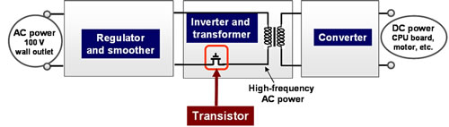 Figure 1. Schematic view of power supply
Larger View (49 KB)
Transistors made of materials with high breakdown-voltages(7) are effective in reducing on-state loss - this is attributable to the fact that transistors made with high breakdown-voltages can be designed with closely spaced electrodes, resulting in lower power loss when passing current. GaN HEMTs are one type of transistor featuring high breakdown-voltage that has attracted much attention in recent years. GaN HEMTs have less than one-fifth (1/5) the on-state loss of silicon transistors and have excellent high-speed characteristics, so that switching losses are less than 1% of those of silicon transistors.
Technological Challenges
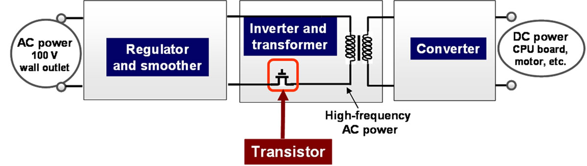
 Figure 2. GaN HEMT structure developed by Fujitsu in 2008 for wireless communication base station amplifiers
Larger View (172 KB)
A desirable characteristic for power supplies used in products such as PCs, home appliances, and automobiles is a complete current-interruption in stand-by mode, in which no voltage is being applied to the gate electrodes. Conventional GaN HEMTs have required a negative gate voltage to be applied when in stand-by mode. In 2008, Fujitsu Laboratories developed a new 3-layer cap structure for GaN HEMTs - by sandwiching an aluminum-nitride (AlN) layer between n-type GaN layers - which can suppress the current when in stand-by (Figure 2). The new GaN HEMT structure was originally developed for wireless transmission amplifiers; however, because the voltage that was applied at the gate electrode in order to switch between on and off states ("turn-on voltage") was in the range of 0.5 V, it could not be used for power supplies, which need to apply +2 to +4 V in order to apply hundreds of volts at the drain. In addition, power supplies effectively need to have an on-state current density of at least 600 milli-amps/millimeter (600 mA/mm).
Newly-Developed Technology
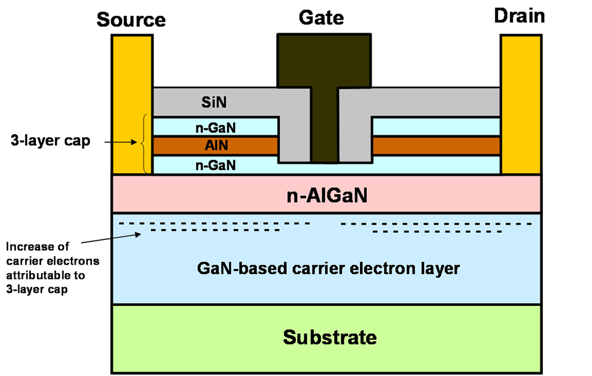
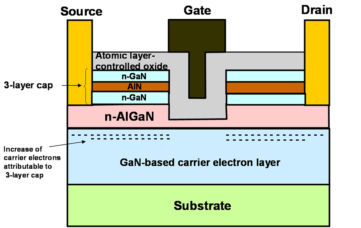
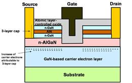 Figure 3. Fujitsu's new GaN HEMT structure for power supply
Larger View (185 KB)
In addition to its GaN HEMT with the three-layer (3-layer) cap structure, Fujitsu made the two following advances in GaN HEMT technology (Figure 3).
- A technology was developed for precise removal of the cap layers and a part of the AlGaN layer only below the gate electrode. By leaving a thin n-type AlGaN layer on the GaN carrier layer, while suppressing damage to the GaN layer, on-state voltage can be increased beyond +2 V while preserving the total interruption in stand-by, enabling high-speed performance when turned on.
- A gate structure was developed that uses an insulated gate structure with an atomic layer-controlled oxide film having atom-level flatness. Because this suppresses gate leak current in which travelling electrons flow to the gate electrode when turned on, a positive voltage can be applied to the gate electrode, resulting in high on-state current density.
Results
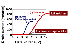 Figure 4. Transistor characteristics of Fujitsu's new GaN HEMT
Larger View (213 KB)
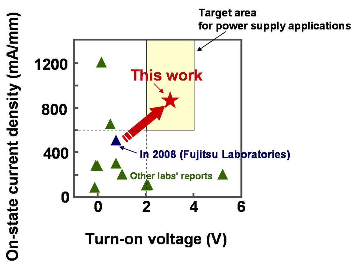
The on-state voltage of the new transistor (Figure 3) reaches +3 V, which can easily be applied to power supplies while achieving a current density of 829 mA/mm - double that of the transistor design on which the new transistor is based (Figure 2) - results in high current values (Figure 4). Among transistors that can achieve an on-state voltage of at least +2 V and completely interrupt current when off, Fujitsu's new transistor features the world's highest on-state current density, making it the first GaN HEMT in the world that has the characteristics required for power supply (Figure 5).
 Figure 5. Maximum current density and turn-on voltage (threshold voltage) benchmarks for Fujitsu's new GaN HEMT (transistors with a breakdown-voltage of 100 V or higher in which current can be interrupted during stand-by without applying a negative gate voltage)
Larger View (88 KB)
With the new transistor in power supplies, power loss can be reduced to one-third (1/3) that of power supplies based on conventional silicon transistors. Extrapolated to all of the data centers in Japan - and taking into account the knock-on benefits of energy savings enabled through reduced air-conditioning electricity required for cooling - this development would reduce data-center power consumption in Japan by 12%, which could be expected to reduce Japan's total CO2 emissions by 330,000 tons(8).
Additionally, the high-frequency performance of Fujitsu's new transistors would enable more compact power supplies. High-speed transistor operation would allow for more compact coils and transformers, which have been particularly difficult to miniaturize in conventional power supplies with low-frequency operation: the size of AC adapters for notebook PCs, for example, could be reduced to one-tenth current sizes. Smaller power supplies would contribute to reducing pace requirements for data centers, as well.
Future Developments
Fujitsu is progressing with practical implementations of GaN transistors featuring high breakdown-voltages, with the aim of producing power supplies based on them by approximately 2011.
-
[1] Gallium-nitride high electron-mobility transistors (GaN HEMT)
A type of transistor with a wide band gap (semiconductors with broad energy bands where electrons cannot reside in the semiconductor's crystalline structure). Tolerates higher voltages than conventional silicon and gallium arsenide (GaAs) semiconductors without breaking down.
-
[2] High electron mobility transistor (HEMT)
A field-effect transistor that takes advantage of operation of the electron layer at the boundary between different semiconductor materials that is relatively rapid compared to that within conventional semiconductors. Invented in 1979 by Dr. Takashi Mimura (currently a Fellow at Fujitsu Laboratories), this technology is currently widely used in various IT applications, including satellite transceivers, mobile phones, GPS-based navigation systems, and broadband wireless networking systems.
-
[3] On-state current
The drain current flowing through a transistor in the on state. When on-state current is low (i.e. high on-state resistance) on-loss rises, resulting in increased power loss.
-
[4] Green Policy Innovation
A global initiative by Fujitsu since November 2007 to help its customers reduce their environmental burden footprint, based on "of IT, for IT".
-
[5] On-state loss
Power loss incurred by a transistor when on, caused by resistance when a transistor is on (on-state resistance).
-
[6] Switching loss
Power loss incurred by a transistor when switching from an on state to an off state. Power loss increases when switching speed is slow.
-
[7] Breakdown-voltage
Maximum voltage that can be applied across the gate and drain electrodes in a transistor. Applying a voltage in excess of this level will destroy the transistor.
-
[8] Reduce data center power consumption by 12%, which could be expected to reduce Japan's total CO2 emissions by 330,000 tons
If GaN HEMTs were used for transistors in power supplies at data centers in Japan, power consumption by servers would be reduced by 8%, and power consumption for air conditioning would be reduced by 4%, resulting in a total reduction of consumed power by 12%. As a whole, data centers in Japan collectively consume 7.72 billion kWh (source: report issued by Japan's Ministry of Internal Affairs and Communications in April 2008, "Study Group on ICT Policy for Addressing Global Warming Report") and a 12% reduction of that figure - converted to CO2 emissions - is 330,000 tons.
About Fujitsu Laboratories
Founded in 1968 as a wholly owned subsidiary of Fujitsu Limited, Fujitsu Laboratories Limited is one of the premier research centers in the world. With a global network of laboratories in Japan, China, the United States and Europe, the organization conducts a wide range of basic and applied research in the areas of Multimedia, Personal Systems, Networks, Peripherals, Advanced Materials and Electronic Devices. For more information, please see:http://jp.fujitsu.com/group/labs/en/
Technical Contacts
Advanced Devices Lab.Devices & Materials Lab.
![]() Phone: +81(46)250-8243
Phone: +81(46)250-8243
![]() E-mail: gan-power-hemt@ml.labs.fujitsu.com
E-mail: gan-power-hemt@ml.labs.fujitsu.com
Company:Fujitsu Laboratories Ltd.
Company and organization names referenced herein are trademarks or registered trademarks of their respective owners. Information provided in this press release is accurate at time of issue and is subject to change without advance notice.
Date: 24 June, 2009
City: Kawasaki, Japan
Company:
Fujitsu Laboratories Ltd.,
,
,
,
,