![]()
Archived content
NOTE: this is an archived page and the content is likely to be out of date.
Fujitsu Laboratories Develops High-Efficiency Gallium-Nitride HEMT Power Amplifier Featuring World's Highest Output Power
- Delivers world's highest output power of 320W and 60% efficiency of power conversion -
Fujitsu Laboratories Ltd.
Fujitsu Laboratories Ltd. announced today the development of a new high-efficiency, high-output amplifier based on gallium-nitride (GaN)(1)high electron mobility transistors (HEMTs)(2) that produces over 300 watts (300W) of power in the C band(3), with 60% efficiency(4) as a ratio of DC input power converted to high-frequency output power. Use of GaN HEMT technology increases output power over existing amplifiers using gallium-arsenide (GaAs) transistors (comparison by Fujitsu Laboratories) by more than six-fold, to 320W. This is expected to extend radar detection range by 2.4 times. It is anticipated that replacing the traveling-wave tube amplifiers(5) commonly used for high output power applications with this new technology will enable smaller, lighter, more energy-efficient, and longer-lasting transmission systems for applications including satellite communications, next-generation mobile phone base stations and radar.
Details of the new technology were presented at the 2008 IEEE Compound Semiconductor IC Symposium (CSICS), held in Monterey, California from October 12 - 15.
Background
In order to increase the capacity of satellite communication transmissions and extend radar detection range, there is a need for high output power of microwave(6) transmitters. Conventional high power microwave transmitters have used traveling-wave tube amplifiers and solid-state amplifiers(7). Due to the fact that traveling-wave tube amplifiers are built around vacuum tubes, they have shorter life spans than solid-state devices and are relatively large and heavy because they require high-voltage power sources. High output power solid-state amplifiers based on GaAs transistors, on the other hand, can provide only low output power from a single element due to their low breakdown voltage, thus requiring composite output from many transistors to achieve adequate transmission power. The loss attributable to this composite circuitry results in reduced efficiency. Thus, development of amplifiers using GaN HEMTs, which feature higher output power and better heat dissipation than GaAs transistors, has been underway in recent years.
Technological Challenge
Transistor chips for high-output-power amplifiers are configured with multiple transistors arrayed in parallel. With a single input and output, the signal that moves along the chip center and the signal that moves along the edges traverse different lengths of wired lines, inducing a phase difference. The result is that the transistors are operating out of phase with each other, making it difficult to fully maximize the high output power characteristics inherent in the transistors.
Newly Developed Technology
The new GaN HEMT-based amplifier (Figure 1) Fujitsu Laboratories has developed is comprised of two transistor chips which resolve the aforementioned technological issue, while producing high output. Key features of the new C-band GaN HEMT-based amplifier include the following:
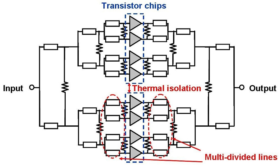
- Employs multi-divided input pathways to prevent occurrence of phase differences to the input signal between the transistors (Figure 2). This enables GaN HEMTs with high output power densities to operate uniformly and efficiently combine their output power.
- The use of two chips can at times create undesirable thermal interference and raise temperatures, thus reducing transistor output. To prevent this, the two chips are spaced a suitable distance from each other, thereby suppressing mutual interference.
These technologies enable the transistors to operate uniformly and to maximize the full high-output power potential inherent in GaN HEMTs.
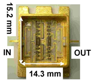 Figure 1: The newly developed C-band amplifier
Larger View (188 KB)
 Figure 2: Structure of the amplifier circuit
Larger View (180 KB)
Results
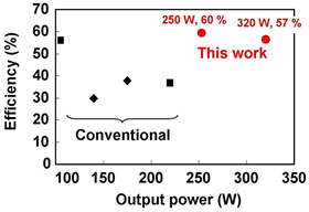 Figure 3: Comparison of power and efficiency for C-band power amplifiers exceeding 100W
Larger View (137 KB)
Fujitsu Laboratories developed two C-band GaN HEMT amplifiers with excellent characteristics - one that features 320W output power with 57% efficiency, another featuring 250W output power with 60% efficiency, both which feature the world's highest output performance for the C-band and which significantly outperform the best previously-reported performance for high-output amplifiers above 100W, which was 220W per package (Figure 3). The 320W amplifier exceeds the output power of conventional GaAs amplifiers more than 6-fold (comparison by Fujitsu), which will enable the extension of wave transmission ranges by 2.4 times.
It is anticipated that traveling-wave tube amplifiers typically used in high-output applications can be replaced by this newly developed GaN HEMT technology, enabling smaller, lighter, more energy-efficient, and longer-lasting transmission systems for such applications as satellite communications, next-generation mobile phone base stations and radar.
Future Developments
Fujitsu Laboratories anticipates that this technology will find broad applications as a replacement for traveling-wave tube amplifiers used in applications requiring high output power and high efficiency, such as wireless communication devices and radar.
For more information:
-
[1] Gallium nitride (GaN)
A wide band-gap semiconductor that features stronger resistance against breakdowns that can occur due to high voltages, compared to conventional semiconductors based on silicon (Si) or gallium arsenide (GaAs).
-
[2] High electron mobility transistor (HEMT)
Invented in 1979 by Takashi Mimura of Fujitsu Laboratories (currently a Fellow at Fujitsu Laboratories), this is a transistor made of compound semiconductors that features excellent operating speed and low noise characteristics. Fujitsu led the industry with its development of the HEMT in 1980, and the technology now underpins much of today's fundamental IT infrastructure, including satellite transceivers, wireless equipment, GPS-based navigation systems, and broadband wireless networking systems.
-
[3] C-band
Name for the frequency band from 4 to 8 GHz. This band is relatively unaffected by rainfall and fog. Applications include satellite communications, fixed wireless communications, wireless access, air-traffic control radar, and weather radar.
-
[4] Efficiency
An index that expresses the ratio of DC input power converted to high-frequency output power.
-
[5] Traveling-wave tube amplifier
A type of vacuum tube used to amplify microwaves. It creates an electron beam that travels at approximately the same speed as the microwave's phase velocity, modulating the speed and density of the electron beam, and amplifying the microwave through a synergistic action between the two.
-
[6] Microwave
Refers to electromagnetic waves with frequencies between 30 MHz and 30 GHz.
-
[7] Solid-state amplifier
An amplifier constructed with silicon- (Si) or gallium arsenide- (GaAs) based semiconductors as active elements.
About Fujitsu Laboratories
Founded in 1968 as a wholly owned subsidiary of Fujitsu Limited, Fujitsu Laboratories Limited is one of the premier research centers in the world. With a global network of laboratories in Japan, China, the United States and Europe, the organization conducts a wide range of basic and applied research in the areas of Multimedia, Personal Systems, Networks, Peripherals, Advanced Materials and Electronic Devices. For more information, please see:http://jp.fujitsu.com/group/labs/en/
Technical Contacts
Advanced Devices Lab.Devices & Materials Lab.
![]() Phone: +81(462)50-8229
Phone: +81(462)50-8229
![]() E-mail: gan-hemt-press@ml.labs.fujitsu.com
E-mail: gan-hemt-press@ml.labs.fujitsu.com
Company:Fujitsu Laboratories Ltd.
Company and product names referenced herein are trademarks or registered trademarks of their respective owners. Information provided in this press release is accurate at time of publication and is subject to change without advance notice.
Date: 21 October, 2008
City: Kawasaki, Japan
Company:
Fujitsu Laboratories Ltd.,
,
,
,
,