![]()
Archived content
NOTE: this is an archived page and the content is likely to be out of date.
Fujitsu Laboratories Develops Low-power CMOS Technology For 32nm Generation
- Minimizes Increase in Number of Manufacturing Processes -
Fujitsu Laboratories Ltd.,Fujitsu Microelectronics
Fujitsu Laboratories Ltd. and Fujitsu Microelectronics Limited today announced the development of low-power CMOS(1) technology for 32nm-generation logic LSIs, which makes it possible to minimize the number of necessary manufacturing processes for LSIs, and without the need to utilize additional new materials. While minimizing rising costs associated with a rise in additional manufacturing processes, the newly developed technology can reduce power-supply voltage without causing a drop in operation speeds, and can lower operational power consumption by approximately 40% compared to technologies for 45nm-generation logic LSIs. It is anticipated that this new technology can be used for wide range of applications, such as for system LSIs for mobile devices which are becoming increasingly multi-functional, and microprocessors that are increasingly adopting multi-core configurations.
Details of this technology will be presented at the 2008 Symposium on VLSI Technology, to be held from June 17 to June 19 in Honolulu, Hawaii.
Background
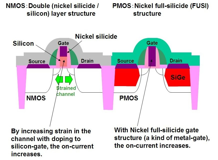
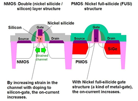 Figure 1: 32nm-generation low-power CMOS technology
Larger View (266 KB)
Reducing power-supply voltage is an effective means of reducing power consumption in NMOS(2) and PMOS(3) transistors, the basic devices of logic LSIs. However, simply lowering power-supply voltage decreases the on-current that a MOS transistor can supply, thus leading to a drop in operation speed. In response to this problem, it is expected that various companies are planning to use metal for gate electrode material as a promising alternative to a conventional silicide/silicon structure, with the aim of achieving high speed and low power consumption in 32nm logic LSIs which are slated for deployment around 2010. A metal gate electrode can significantly increase the on-current that a MOS transistor can supply, thereby enabling a logic LSI to consume less power without degrading operating speed.
Technological Challenges
With metal gate electrodes for 32nm-generation logic LSIs, to achieve on-current equivalent to that of previous levels even while using low voltage, NMOS and PMOS devices must have different metal materials for their gate electrode, thus leading to a rise in costs due to the necessitation of new materials and the need for additional manufacturing processes.
Newly Developed Technology
By developing new technology for both NMOS and PMOS devices, and by minimizing the need for new materials or an increase in additional manufacturing processes, Fujitsu Laboratories succeeded in lowering power consumption without degrading operating speed, on par with other 32nm metal gate technologies reported thus far.
Key features of the new technology are as follows:
- Double-layer gate technology for NMOS
For the NMOS device, the new technology uses a conventional double-layer gate-electrode structure consisting of a nickel-silicide(4) layer and a silicon layer, but adds impurities to the silicon layer. This adds a large amount of strain to the channel region where on-current flows thereby increasing the on-current. As a result, the device can be operated with less power without degrading operating speed. - Nickel fully silicided gate technology for PMOS
By employing high-temperature heat treatment and optimized structures, the technology makes it possible to fully silicide(5) just the PMOS gate electrode, by using nickel which has been widely used in the past as a silicide material. Because this gate electrode based on nickel silicide functions as a metal gate electrode, there are no remarkable drops in performance due to depletion(6) in the gate electrode - a common problem for conventional silicide/silicon gate PMOS in particular - and as a result, on-current can be increased. Thus, this PMOS nickel fully-silicided gate technology enables low-power operation without degradation of operation speeds compared to 45nm logic LSIs.
Results
By utilizing this new technology, it was possible to significantly reduce the number of necessary new manufacturing process from six to just one process, compared to 32nm-generation metal gate technologies that were previously reported. As a result, cost increase was limited to less than 1% technology in comparison with other 32nm metal gate technology.
In terms of performance, on par with other 32nm metal gate technologies, the new technology can lower power-supply voltage without a drop in operating speed compared to 45nm logic LSIs and thus reduces operational power consumption by approximately 40%.
Future Developments
Through developments of related technologies, Fujitsu aims to enable low-power 32nm-generation technology applications.
-
[1] CMOS
Complementary metal-oxide semiconductor.
-
[2] NMOS
Negative-channel metal-oxide semiconductor.
-
[3] PMOS
Positive-channel metal-oxide semiconductor.
-
[4] Nickel silicide
Silicide is a chemical compound consisting of silicon and a high-melting-point metal such as cobalt or titanium in addition to nickel.
-
[5] Fully silicided
A gate structure in which the whole gate electrode is made of silicide.
-
[6] Depletion
Decrease in the number of free carriers in the section bordering the gate oxide film within the gate electrode when applying gate voltage. Electrically speaking, it is equivalent to an increase in the thickness of the gate oxide film, which causes a decrease in on-current.
About Fujitsu Laboratories
Founded in 1968 as a wholly owned subsidiary of Fujitsu Limited, Fujitsu Laboratories Limited is one of the premier research centers in the world. With a global network of laboratories in Japan, China, the United States and Europe, the organization conducts a wide range of basic and applied research in the areas of Multimedia, Personal Systems, Networks, Peripherals, Advanced Materials and Electronic Devices. For more information, please see:http://jp.fujitsu.com/group/labs/en/
About Fujitsu Microelectronics (FML)
Fujitsu Microelectronics Limited (FML) is a large-scale integrated circuit (LSI) manufacturer that provides highly reliable, optimal solutions to meet the varying needs of its customers, through LSI offerings including ASIC/COT, ASSP and power management ICs, and flash microcontrollers. Along with building on its wide-range expertise focusing on imaging, wireless, and security LSI applications, FML also pursues initiatives for power efficiency and undertakes environmentally-conscious countermeasures. Headquartered in Tokyo, FML was established as a subsidiary of Fujitsu Limited on March 21, 2008. Through its global sales and development network with sites in Japan and other regions in Asia, Europe, and the U.S., FML offers LSI solutions to the global marketplace. For more information:http://jp.fujitsu.com/group/fml/en/
Technical Contacts
Silicon Technologies Development Lab.
![]() Phone: +81-594-24-2294
Phone: +81-594-24-2294
![]() E-mail: silicon-ask@ml.labs.fujitsu.com
E-mail: silicon-ask@ml.labs.fujitsu.com
Company:Fujitsu Laboratories Limited
Company and product names referenced herein are trademarks or registered trademarks of their respective owners. Information provided in this press release is accurate at time of publication and is subject to change without advance notice.
Date: 17 June, 2008
City: Kawasaki and Tokyo
Company:
Fujitsu Laboratories Ltd.,
Fujitsu Microelectronics Limited,
,
,
,