![]()
Archived content
NOTE: this is an archived page and the content is likely to be out of date.
Fujitsu Develops Technology for Low-Power, High-Performance 45nm Logic Chips
Incorporates new annealing technology and multi-layer interconnect technology
Fujitsu Limited,Fujitsu Laboratories Ltd.
Fujitsu Limited and Fujitsu Laboratories Ltd. today announced their development of a platform technology for 45 nanometer (45nm) generation LSI logic chips, which combines technologies for low power consumption and high-performance interconnect. Compared to previous 45nm technologies on record, the new platform reduces the leakage current that occurs when current is wasted in wait states to one-fifth that of previous levels and reduces interconnect-induced lag times by approximately 14%. The realization of these new 45nm generation platform technologies will enable Fujitsu to offer its customers LSI logic chips that feature even higher speeds, smaller size and lower power consumption than currently available.
Details of the new technology were presented at the 2007 Symposium on VLSI Technology.
Background
The need to achieve higher levels of integration in LSI logic chips is becoming greater, spurred by the higher level of performance needed to support the proliferation of functions in various devices, and the need for multiple processor cores on devices. In light of these trends, for 45nm generation logic technology, in accordance with higher integration levels and enhancements in performance speeds, technologies able to suppress power consumption of devices are becoming increasingly important.
In order to heighten integration levels of LSIs, with each new generation of devices, there is a need to shorten the gate length of each transistor and make the spaces between interconnects narrower. In addition, to achieve high speeds there is a need to minimize the time lag from interconnects between the hundreds of millions of individual transistors within the LSI chip (Figure 1).
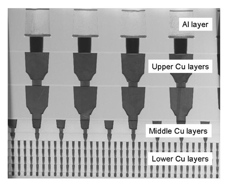 Figure 1: Cross-section of 9Cu + 1Al interconnect module with Full-NCS at lower Cu layers, developed by Fujitsu
Larger View (100 KB)
Technological Challenges
When a the gate length of a transistor is shortened, a problem that exists is increased power consumption attributable to increased leakage current between the transistor's source and drain when no signal voltage is applied at the gate - for example, when a mobile phone is on standby mode awaiting calls and no operation processing is underway.
For the 45nm generation, both the width of interconnects and the spaces between interconnects, are at the smallest 65nm. In addition to an increase of interconnect resistance due to miniaturization, if the insulating layer's dielectric constant stays the same as the previous generation, interconnect capacitance will increase, thereby resulting in increased interconnect lag and thus necessitating a material with lower dielectric constant.
Fujitsu's New Technology
1. New annealing technology
Fujitsu researchers found that forming shallower source and drain regions is an effective way to reduce leakage current (Figure 2). However, simply making them shallower also increases resistance at the source and drain regions, thereby degrading transistor performance. To counteract this, Fujitsu researchers developed a new annealing technology called millisecond annealing (MSA). Compared to previous annealing, Fujitsu's millisecond annealing technology uses higher temperatures thus enabling reduction of resistance, and because the annealing time is brief it possible to form shallow sources and drain regions and thereby reduce leakage current.
2. High-performance interconnects
Fujitsu researchers used nano-clustering silica (NCS), which has a dielectric constant (k) of 2.25 - the lowest of any insulating film reported to date - in a lower interconnect region suitable for the smallest interconnect spaces.
NCS is an insulating material pocked with miniscule holes, enabling both a low dielectric value and high mechanical strength simultaneously. Fujitsu introduced NCS on a partial basis beginning with the 65nm generation. However, for the 45nm generation, the company is using NCS not just within a given interconnect layer but also between different layers to further reduce interconnect capacitance.
Results
The new annealing technique is highly effective in limiting transistor resistance, reducing leakage current to one-fifth that of previous levels, thereby enabling advantages such as extending mobile phone maximum standby (wait) time up to five-fold.
In addition, by utilizing high-performance interconnect technology Fujitsu was able to achieve a 14% reduction in interconnect lag time in comparison to standard 45nm generation interconnect technologies in the International Technology Roadmap for Semiconductors(1).
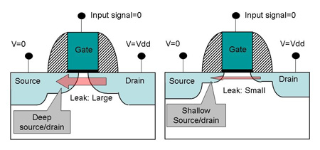 Figure 2: Relation between source/drain junction depth and leak current
Larger View (119 KB)
Future Developments
These two newly developed technologies enable the reduction of leakage current during standby, while simultaneously increasing operating speed. Fujitsu is targeting 2008 to incorporate these technologies into LSIs that are suited for mobile devices as part of a ubiquitous networking society.
For more information:
-
[1] International Technology Roadmap for Semiconductors (ITRS)
Known as ITRS, this roadmap for semiconductors is sponsored by five leading semiconductor manufacturing regions in the world: Japan, the United States, Europe, Korea, and Taiwan. The sponsoring organizations are the Japan Electronics and Information Technology Industries Association (JEITA), the United States Semiconductor Industry Association (SIA), the European Semiconductor Industry Association (ESIA), the Korean Semiconductor Industry Association (KSIA), and the Taiwan Semiconductor Industry Association (TSIA). For more information:http://www.itrs.net/about.html
About Fujitsu
Fujitsu is a leading provider of customer-focused IT and communications solutions for the global marketplace. Pace-setting device technologies, highly reliable computing and communications products, and a worldwide corps of systems and services experts uniquely position Fujitsu to deliver comprehensive solutions that create infinite possibilities for its customers' success. Headquartered in Tokyo, Fujitsu Limited (TSE:6702) reported consolidated revenues of 5.1 trillion yen (US$43.2 billion) for the fiscal year ended March 31, 2007. For more information, please see: www.fujitsu.com
About Fujitsu Laboratories
Founded in 1968 as a wholly owned subsidiary of Fujitsu Limited, Fujitsu Laboratories Limited is one of the premier research centers in the world. With a global network of laboratories in Japan, China, the United States and Europe, the organization conducts a wide range of basic and applied research in the areas of Multimedia, Personal Systems, Network, Peripherals, Advanced Materials and Electronic Devices. For more information, please see: http://jp.fujitsu.com/labs/en/
Technical Contacts
Silicon Technologies Development Lab.
![]() Phone: +81-42-532-1253
Phone: +81-42-532-1253
![]() E-mail: silicon-ask@ml.labs.fujitsu.com
E-mail: silicon-ask@ml.labs.fujitsu.com
Company:Fujitsu Laboratories Ltd.
Company names mentioned herein are registered trademarks or trademarks of their respective owners. Information provided in this press release is accurate at time of publication and is subject to change without advance notice.
Date: 18 June, 2007
City: Tokyo
Company:
Fujitsu Limited,
Fujitsu Laboratories Ltd.,
,
,
,