![]()
Archived content
NOTE: this is an archived page and the content is likely to be out of date.
Tokyo Institute of Technology and Fujitsu Laboratories Actualize World's First Infrared Light Propagation in Optical Crystal Films on Silicon Substrate
-New technology paves the way for ultra-compact optical communication devices-
Tokyo Institute of Technology,Fujitsu Laboratories Ltd.
The Tokyo Institute of Technology and Fujitsu Laboratories Limited today announced their joint development of a new technology that enables the successful propagation of infrared light through an optical crystal film on a silicon substrate, for the first time in the world. The technology is a result of collaborative development by the laboratory of Associate Professor Kazuo Shinozaki of the Tokyo Institute of Technology and Fujitsu Laboratories, and paves the way for compact optical communication devices featuring the integration of silicon large-scale integrated circuits (LSIs) with various optical devices such as modulators and switches.
The new technology was developed to lead the future of ultra-compact optical communications systems, and was enabled by the matching funds from the initiative known as the Effective Promotion of Joint Research with Industries, Academia and Government, from the Special Coordination Funds for Promoting Science and Technology provided by the Ministry of Education, Culture, Sports, Science and Technology of the government of Japan.
Details of the technology will be presented at The 24th Meeting on Ferroelectric Materials and Their Applications (FMA-24) to be held in Kyoto, Japan from May 23, and at the International Symposium on the Application of Ferroelectrics (ISAF2007) to be held in Nara, Japan from May 27.
Background
Today's ubiquitous networking society increasingly demands smaller sizes and lower costs for high-speed large capacity optical communications systems. Currently available optical communications systems are comprised of devices for processing of optical signals, and silicon LSI devices for processing electrical signals, which are manufactured and assembled separately. The realization of a compact optical transmission device in which the two separate types of devices are integrated would enable further downscaling and lower costs for optical communication systems.
Technological Challenges
In order to enable the use of communications devices such as optical switches and modulators on a silicon substrate, a material with electro-optic effect(1) must be formed on the substrate and light must be propagated through that material. One material known to have excellent electro-optic coefficient is the ferroelectric(2) material, lead zirconate titanate (PZT(3)). However, due to the fact that significant loss of propagation is incurred due to disruption of crystals when single crystal film is formed on top of silicon substrate, it had thus far been difficult to propagate light successfully.
Overview of the New Technology
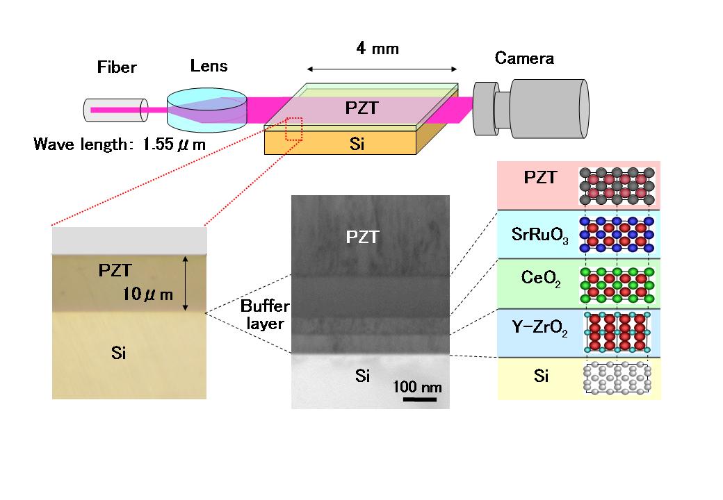
To overcome the aforementioned technical issue, a buffer layer with a three-layer structure(4)(Ref: Figure 1) was utilized on the surface of a silicon substrate, and a PZT single crystal film was formed over the layer. This enabled minimization of the disruption of the atomic alignment, thereby resulting in a high-quality ferroelectric PZT single-crystal-film with proper atomic alignment, and also prevented reaction between the PZT and silicon.
 Figure 1: Schematic of infrared propagation experiment
Larger View (67 KB)
Results
With the same wavelength of infrared light typically used in optical communications (1.55 microns), Tokyo Institute of Technology and Fujitsu Laboratories successfully minimized the PZT propagation loss to less than one decibel per centimeter (1dB/cm) which is approximately one-tenth (1/10) the loss that had been incurred with existing technologies.
The parties also succeeded in demonstrating the world's first successful propagation of infrared light through an optical crystalline film formed on a silicon substrate.
The electro-optic coefficient(5), a figure representing the level of change in the refractive index, was verified as being 76 picometers per volt (76pm/V) with infrared light. This is approximately three times the value of lithium niobate single crystals, which are widely used as optical modulators.
Future Developments
Fujitsu Laboratories and the Tokyo Institute of Technology will utilize this new crystal-forming technology for the development of technologies to form various optical devices on silicon substrates.
For more information:
-
[1] Electro-optic effect
A characteristic in which the refractive index changes when voltage is applied.
-
[2] Ferroelectric material
A material capable of reversing its polarity when voltage is applied. This polarization inversion is used in various applications such as memory and piezoelectric actuators.
-
[3] PZT
Lead zirconate titanate. Formula: Pb(Zr,Ti)O3. Oxidized compound of lead, zirconium, and titanium. Well-known as a ferroelectric material and widely used in a broad range of applications across various fields.
-
[4] Three-layer structure
Three-layer structure comprised of the following: strontium ruthenium oxide: SrRuO3(132nm), ceria: CeO2(52nm), and yittria-stabilized zirconia: Y-ZrO2(64nm).
-
[5] Electro-optic coefficient
A coefficient that expresses the level of change incurred in a refractive index when voltage is applied. The higher a value is, the larger the level of change of the refractive index.
About Fujitsu Laboratories
Founded in 1968 as a wholly owned subsidiary of Fujitsu Limited, Fujitsu Laboratories Limited is one of the premier research centers in the world. With a global network of laboratories in Japan, China, the United States and Europe, the organization conducts a wide range of basic and applied research in the areas of Multimedia, Personal Systems, Networks, Peripherals, Advanced Materials and Electronic Devices. For more information, please see:http://jp.fujitsu.com/group/labs/en/
Press Contacts
Center for Public Relations and CoordinationNational University Corporation Tokyo Institute of Technology
![]() Phone: +81-3-5734-2975
Phone: +81-3-5734-2975
Fax: +81-3-5734-3661
![]() E-mail: kouhou@jim.titech.ac.jp
E-mail: kouhou@jim.titech.ac.jp
Company:Tokyo Institute of Technology Press Contact
Technical Contacts
Shinozaki LaboratoryDepartment of Metallurgy and Ceramics Science
Graduate School of Science and Engineering
National University Corporation
Tokyo Institute of Technology
![]() Phone: +81-3-5734-2518
Phone: +81-3-5734-2518
![]() E-mail: info@sim.ceram.titech.ac.jp
E-mail: info@sim.ceram.titech.ac.jp
Company:Tokyo Institute of Technology Technical Contact
Technical Contacts
Device and Materials LaboratoriesFujitsu Laboratories Ltd.
![]() Phone: +81-46-250-8362
Phone: +81-46-250-8362
![]() E-mail: msl@ml.labs.fujitsu.com
E-mail: msl@ml.labs.fujitsu.com
Company:Fujitsu Technical Contact
Company and other organizational names referenced herein are trademarks or registered trademarks of their respective owners. Information provided in this press release is accurate at time of publication and is subject to change without advance notice.
Date: 29 March, 2007
City: Tokyo
Company:
Tokyo Institute of Technology,
Fujitsu Laboratories Ltd.,
,
,
,