Archived content
NOTE: this is an archived page and the content is likely to be out of date.
Fujitsu Develops World's First CMOS Selector Chip Operating at 50 Gbps
Fujitsu Limited,Fujitsu Laboratories Ltd.
Tokyo, March 23, 2004
Fujitsu Laboratories Ltd. and Fujitsu Limited today announced the development of a selector chip (*1) using Fujitsu's CMOS technology capable of record-breaking 50-Gbps throughput. The new technology delivers the benefits of a highly integrated, low-power design in CMOS with the 40-Gbps performance levels required for devices used in high-bandwidth data communications, speeds that previously could only be attained using silicon-germanium chips or other compound semiconductors.
This technology represents a breakthrough in achieving the 40-Gbps throughput levels required of devices for next-generation telecommunications. Details of the new technology were presented last month at the International Solid-State Circuit Conference.
Background
With the ongoing spread of broadband Internet access, there is a growing need for networks that can deliver higher speeds and bandwidth capacity. Although the current standard is 10 Gbps, next-generation network systems need to be able to run at 40 Gbps. Reaching those speeds will require ultra-fast chips that can process data at rates of at least 40 Gbps, and most development work has focused on silicon-germanium and other compound semiconductors that offer superior speed characteristics.
Technological Challenges
But while devices using silicon-germanium or other compound semiconductors can offer superior speed, they consume very high levels of power, posing heat problems for highly integrated designs, and are expensive in terms of manufacturing costs. CMOS chips, on the other hand, consume less energy and cost less, but the transistor characteristics and interconnect parasitic capacitances of CMOS chips have-with the approaches pursued up until now-made it difficult achieve speeds exceeding 40 Gbps.
Fujitsu's Technology
Fujitsu's new technology enables CMOS circuits to operate faster. With a new circuit schematic employing inductors (*2) and cutting-edge 90-nm CMOS technology, Fujitsu was able to achieve a dramatic increase in processor throughput. The key features of the new technology are as follows:
- Inductor peaking
To eliminate the factors within the circuit relating to transistors and interconnect parasitic capacitances that inhibit high-speed operation, Fujitsu placed an inductor at an optimized location on each circuit, achieving a breakthrough in operating speed. The inductor is a 3-µm copper trace formed on the top interconnect layer.
- Advanced 90-nm CMOS technology
Building on the current generational standard of 90-nm CMOS technology, Fujitsu used transistors with a reduced gate length of 48 nm and optimized the circuit parameters to maximize the chip performance.
- Highly precise modeling
Fujitsu developed a modeling methodology that, across the range from low-frequency operation to high-frequency, precisely corresponds to each element of the circuit, including the transistor, inductor, and interconnect. This methodology enabled highly precise circuit simulation, resulting in an optimized circuit design even with the inclusion of the novel inductor circuit structure.
Results
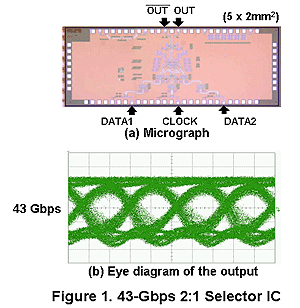
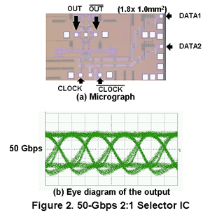
Fujitsu developed two selector chips with different circuit schematics using this technology, achieving throughput of 43 Gbps and 50 Gbps, respectively (see Figures 1 and 2). This is the first time that chips using CMOS technology have verifiably achieved operating speeds in excess of 40 Gbps.
The selector chip operating at 50 Gbps uses a circuit schematic that takes 1.0V power, standard for 90-nm CMOS chips, and would be relatively easy to develop into large-scale system-on-chip devices.
Future Developments
Fujitsu is currently developing large-scale system-on-chip devices incorporating this technology, aiming for commercial release some time around 2006 to 2007.
About Fujitsu Laboratories
Founded in 1968 as wholly owned subsidiary of Fujitsu Limited, Fujitsu Laboratories Limited is one of the premier research centers in the world. With a global network of laboratories in Japan, China, the United States and Europe, the organization conducts a wide range of basic and applied research in the areas of Multimedia, Personal Systems, Networks, Peripherals, Advanced Materials and Electronic Devices.
About Fujitsu
Fujitsu is a leading provider of customer-focused IT and communications solutions for the global marketplace. Pace-setting technologies, highly reliable computing and telecommunications platforms, and a worldwide corps of systems and services experts uniquely position Fujitsu to deliver comprehensive solutions that open up infinite possibilities for its customers' success. Headquartered in Tokyo, Fujitsu Limited (TSE:6702) reported consolidated revenues of 4.6 trillion yen (US$38 billion) for the fiscal year ended March 31, 2003.
For more information, please see: www.fujitsu.com
Press Contacts
Public & Investor Relations
Inquiries
Company:Fujitsu Limited
Technical Contacts
System LSI Development Laboratories
Network SOC Development Lab.
 Phone: +81-44-754-2389
 E-mail: sel@ml.labs.fujitsu.com
Company:Fujitsu Laboratories, Ltd.
All company/product names mentioned may be trademarks or registered trademarks of their respective holders and are used for identification purpose only.
Please understand that product prices, specifications and other details are current on the day of issue of the press release, however, may change thereafter without notice.
Date: 23 March, 2004
City: Tokyo
Company:
Fujitsu Limited,
Fujitsu Laboratories Ltd.,
,
,
,
![]() Phone: +81-44-754-2389
Phone: +81-44-754-2389![]() E-mail: sel@ml.labs.fujitsu.com
E-mail: sel@ml.labs.fujitsu.com
