Fujitsu

Global

Archived content

NOTE: this is an archived page and the content is likely to be out of date.

Fujitsu Develops World's First Multi-layer PCB Capable of 5Gbps Transmission and 4000 Pin Mounting

Fujitsu Laboratories Ltd.,Fujitsu Interconnect Technologies Limited,Fujitsu Limited

Tokyo, March 09, 2004

Fujitsu Laboratories Ltd., Fujitsu Interconnect Technologies Ltd., and Fujitsu Limited today announced the joint development of new manufacturing technologies for large-sized, high-count multi-layer printed circuit boards (PCBs) that enable support of 5Gigabits per second (5Gbps) high-speed transmission and 4000 pin high-density mounting (0.8mm pitch). Fujitsu's new technologies succeed in improving manufacturing yields and significantly reducing production time for high-count multi-layer PCBs. The technologies were developed for use in such areas as next-generation, high-speed servers and telecommunication base station equipment, which demand fast transmission speeds and high-density mounting.

Background

With the increasingly higher levels of performance and functionality of computers and telecommunication networking devices, there is demand for large-sized, high-count multi-layer PCBs (e.g. 600 x 600 mm, exceeding 20 layers) capable of data transmission speeds of 5Gbps for telecommunication base stations. Due to advances in CMOS technology, pin-counts of chip packages mounted on PCBs continue to increase, with current maximum pin count of 2500 pins (1mm pitch) to increase to 4000 pins (0.8mm pitch) by 2005. At the same time, there is demand for higher manufacturing yields and shorter production time.

Technological Challenges

Conventionally, large-scale multi-layer PCBs were produced employing a Sequential Lamination Method(1). However, as wiring for high-density mounting cannot be achieved by this method alone, the Sequential Lamination Method was combined with the Build-up Method(2). Although the Build-up Method is effective for high-density mounting of small devices, as repetitive layering is necessary, this method requires more production days in comparison to the Sequential Lamination Method. Low yield was also an issue when using the Build-up Method. Furthermore, due to the fact that high-speed circuits capable of 5Gbps-level transmission suffer damage to their 3-dimensional section of wiring through losses such Via Holes(3), weakened transmission signal problems occur. As conventional circuit simulation was incapable of accurately estimating these losses, there was demand for technologies that could provide accurate estimates of actual transmission loss and improve design precision.

Fujitsu's New Technology

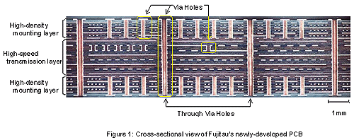
Fujitsu has newly developed two technologies: a manufacturing technology for large-sized, high-count multi-layer PCBs which employs separately producing high-speed transmission layers and high-density mounting layers each as separate individual PCBs and integrating them later; and its accompanying design simulation technology. In addition to enabling both 5Gbps high-speed transmission and 0.8mm pitch high-density mounting, benefiting from this new circuit simulation technology capable of accurate estimates of loss to wiring and the 3-Dimensional section of wiring such as Via Holes, it is now possible to analyze effects of those losses during the design phase.

Features of Fujitsu's newly developed technologies are as follows:

1. Multi-layer PCB manufacturing technology that achieves both high-speed transmission and high-density mounting

A new manufacturing technology for high-count multi-layer PCBs was developed, which entails creating high-speed transmission wiring layers and high-density mounting layers as separate PCBs, and then merging the layers. Although merging of large-scale high multi-layer PCBs requires high-precision positioning accuracy and is thus deemed difficult, Fujitsu has successfully achieved this through technology from Fujitsu Interconnect Technologies' proven expertise in manufacturing of products in this field.

By producing high-speed transmission wiring layers and high-density mounting layers as separate PCBs, it is now possible to use combinations of dielectric materials between layers that are in accordance with desired performance and cost demands. Furthermore, 3-dimensional structuring, a cause for loss during high-speed transmission, has been significantly reduced.

2. Three-dimensional wiring simulation technology

Fujitsu developed simulation technology that accurately estimates transmission losses. Fujitsu has succeeded in deriving accurate estimates at 5Gbps bandwidth of losses that occur in 3-dimensional wiring, by applying effective material parameters(4) derived from highly accurate measuring techniques for transmission loss, to electromagnetic field analysis(5). In addition, by incorporating property parameters derived by the newly developed methods, 3-dimensional wiring can be replaced with inductor (L), capacitor (C) and resistor (R) circuits, and can be handled on conventional circuit simulations.

Results

The newly developed technologies are comprehensive technologies for multi-layer PCBs, spanning from circuit design and board manufacture, to inspection. The new technologies enable both 5Gbps transmission speed and 4000 pin (0.8mm pitch) BGA (Ball Grid Array)(6) mounting for large-scale boards up to 60cm in size. By employing the Sequential Lamination Method for all processes, Fujitsu has achieved: 1) tremendous improvements in yield by conducting quality inspection prior to integration; 2) simplification of the production process; and 3) stronger post-integration durability.

As Fujitsu has enabled accurate estimates of transmission losses that occur to 3-dimensional wiring such as Via Holes, circuit transmission characteristics can now be analyzed during the design phase, thereby significantly improving high-speed transmission circuit design accuracy at 5Gbps bandwith. These advantages reduce the number of times prototypes must be produced during the design stage for transmission characteristic confirmation, resulting in a shorter development period.

Future Developments

Fujitsu will push forward with technology development for large-scale high-count multi-layer PCBs capable of transmission speeds exceeding 10Gbps. In accordance with Fujitsu's environmentally friendly corporate initiative, the newly developed PCB is lead-free, with goals to make it halogen-free. Fujitsu will continue hereafter with product development that is environmentally conscious.

Fujitsu Interconnect Technologies is scheduled to start sample shipments of products utilizing Fujitsu's newly developed technologies from June 2004, with volume production slated for December 2004. Fujitsu Interconnect Technologies anticipates sales of 2 billion yen in its fiscal year 2005 (April 2005 - March 2006).

figure 1

  • [1] Sequential Lamination Method

    A manufacturing method for PCBs in which materials for which wiring patterns have been formed in advance are integrated in a single lamination process, and the layers are connected by a mechanical drill by using ordinary plated Through Via Hole processing.

  • [2] Build-up Method

    A method that enables intricate wiring, by alternately forming dielectric layers and wiring layers on the PCB that functions as the main PCB.

  • [3] Via Holes

    In multi-layer wiring, the connecting sections between layers.

  • [4] effective material parameters

    A physical value unique to each material, such as dielectric constant or dielectric loss, that is necessary for simulation.

  • [5] electromagnetic field analysis

    A method for analyzing various transmission characteristics, through numeric simulation of electromagnetic field-strength distribution within 3-dimensional wiring.

  • [6] BGA (Ball Grid Array)

    One type of mounting methods available in which the IC package and PCB are connected through high-density mounting. Hemispherical input and output terminals are laid in grids on the IC package and then mounted to the PCB.

About Fujitsu Laboratories Limited

Founded in 1968 as wholly owned subsidiary of Fujitsu Limited, Fujitsu Laboratories Limited is one of the premier research centers in the world. With a global network of laboratories in Japan, China, the United States and Europe, the organization conducts a wide range of basic and applied research in the areas of Multimedia, Personal Systems, Networks, Peripherals, Advanced Materials and Electronic Devices. For additional information, please see:
For more information, please see: www.labs.fujitsu.com/en/

About Fujitsu Interconnect Technologies Limited

Fujitsu Interconnect Technologies Limited (FICT), a technology leader in PCB design and manufacturing innovation, is a wholly owned subsidiary of Fujitsu Limited of Japan. FICT's U.S. operations, located in the Silicon Valley, provide innovative design and manufacturing solutions for package substrates and printed circuit boards to meet the needs of its global customer base. FICT's solutions enable its customers to migrate to newer, complex designs, while reducing manufacturing time and total cost.

FICT offers manufacturing services for market segments including computing PCBs such as PCs, servers and media devices; networking PCBs such as switches, routers and storage; module PCBs such as miniature camera applications; consumer PCBs such as cell phones, PDAs, video games; and industrial PCBs such as automotive, medical. FICT also offers design, design review, design enhancement, layer reduction, testing and evaluation services for PCBs from four to 54 layers.
For more information, please see: us.fujitsu.com/fbf/fict/home

About Fujitsu

Fujitsu is a leading provider of customer-focused IT and communications solutions for the global marketplace. Pace-setting technologies, highly reliable computing and telecommunications platforms, and a worldwide corps of systems and services experts uniquely position Fujitsu to deliver comprehensive solutions that open up infinite possibilities for its customers' success. Headquartered in Tokyo, Fujitsu Limited (TSE:6702) reported consolidated revenues of 4.6 trillion yen (US$38 billion) for the fiscal year ended March 31, 2003.  
For more information, please see: www.fujitsu.com

Press Contacts

Inquiries

Company:Fujitsu Limited

Customer Contacts

Phone: Phone: +81-44-754-2260
E-mail: E-mail: fictquery@fict.fujitsu.com
Company:Fujitsu Interconnect Technologies Ltd.

Technical Contacts

Materials and Environmental Engineering Lab.

Phone: Phone: +81-46-250-8834
E-mail: E-mail: me-engineering@labs.fujitsu.com
Company:Fujitsu Laboratories Ltd.

Technical Contacts

Corporate Technology Engineering Center

Phone: Phone: +81-44-754-2189
E-mail: E-mail: me-engineering@labs.fujitsu.com
Company:Fujitsu Limited

Date: 09 March, 2004
City: Tokyo
Company: Fujitsu Laboratories Ltd., Fujitsu Interconnect Technologies Limited, Fujitsu Limited, , ,