![]()
Archived content
NOTE: this is an archived page and the content is likely to be out of date.
Fujitsu Develops Ultra-Low-Power Transceiver Chipset for Next-Generation Optical Transmissions Systems
World's First 50-Gbps Operation of a 4:1 Multiplexer and 1:4 Demultiplexer chipset at less than 1 watt
Fujitsu Laboratories Ltd.
Fujitsu Laboratories Ltd. today announced the development of a new communications chipset that uses Indium Phosphide-based high-electron mobility transistor (InP-HEMT(1)) technology to enable 50-Gbps operation of a 4:1 multiplexer(2) and 1:4 demultiplexer(3) chipset. Fujitsu's newly developed chipset is the world's first to achieve superior signal quality and operating margins in full-rate clocking(4) scheme, with breakthrough low-power consumption of less than 1 watt (70% lower than conventional technology).
This new technology was developed to deliver 40 Gbps throughput levels required of chips for next-generation telecommunications. Details of this technology are being presented at the 2004 IEEE International Solid-State Circuit Conference, being held in San Francisco from February 15.
Background
There is a worldwide push to develop new terabit-class (tera = 1 trillion) optical communications systems that will dramatically raise existing data transmission capacity by 10 to 100 times. To enable such achievements, wavelength-division multiplexing (WDM(5)), which multiplexes multiple 40-Gbps optical signals is recognized as an effective method.
Since WDM requires a quantity of electrical signal-processing circuits equivalent to the number of optical signals that are multiplexed together, as the level of multiplexing increases, so does the overall system's power consumption. As such, there is strong demand for power consumption reduction of the electrical signal-processing circuits that comprise the system.
Technological Challenges
Thus far, the reduction of power consumption without degrading superior signal quality and operating margins had been a daunting issue to overcome for multiplexers and demultiplexers that process high-speed signals as much as 40 Gbps.
Fujitsu's New Technology
Fujitsu's new technology has the following key features:
1. Multi-phase clock technology
New circuit architecture was developed in which the circuit internally generates clock signals with different phases and utilizes them to process data signals. This new architecture ensures superior signal quality without the need for a phase-control circuit. By eliminating the phase-control circuit that required by conventional circuits, Fujitsu succeeded in significantly reducing power consumption.
2. Optimized voltage distribution
Through innovative optimized voltage distribution design focused on transistor size and transistor logic operation, Fujitsu was able to reduce supply voltage to less than half (1.5 volts) the voltage that was conventionally required.
3. InP-HEMT technology
By incorporating InP-HEMT technology, ideal for high-speed performance, full-rate clocking mode was utilized to enable superior signal quality and operating margins. This makes it possible to sync the circuit on the clock signal's trailing edge only, resulting in improved quality of multiplexer output signals and higher demultiplexer operating margins.
Results
Fujitsu's new technology succeeds in delivering high speeds and superior signal quality while benefiting from low power consumption that is expected of CMOS technology. Specifically:
- The chipset operates on the world's lowest power consumption of less than 1 watt (a 70% reduction from conventional technology), while enabling 50 Gbps of throughput, more than adequate for 40-Gbps systems.
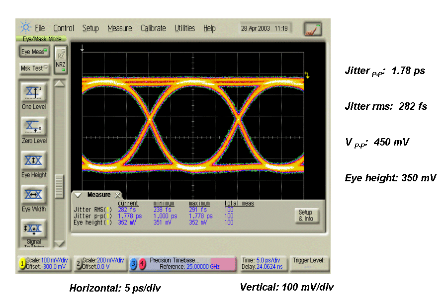
- The 4:1 multiplexer attains the world's highest quality signal in terms of jitter - 284 femtoseconds (femto=one-quadrillionth) - and the 1:4 demultiplexer achieves a clock phase margin of 250 degrees.
By using the newly developed chipset in 40-Gbps optical communications systems, significant reduction of overall system power consumption is anticipated.
Future Developments
Fujitsu plans to leverage this technology to develop circuits such as 16:1 multiplexers and 1:16 demultiplexers that work with 2.5-Gbps interface, a candidate for system standardization, to offer greater performance and higher levels of integration for terabit-class communication systems.

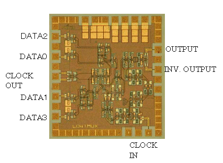
Larger View (62 KB)
Figure 1:
4:1 Multiplexer IC

Larger View (124 KB)
Figure 2:
50-Gbps eye diagram of 4:1 Multiplexer
-
[1] InP-HEMT
Indium Phosphide-based High-Electron Mobility Transistor A field-effect transistor that utilizes the rapid migration (compared to that within conventional semiconductors) of electrons that appear at the joint between semiconducting materials with different band gaps. Using Indium Phosphide in the substrate serves to accelerate the speed of the electrons.
-
[2] multiplexer
A circuit that combines multiple low-speed signals into one high-speed signal, based on time slices. When used in the transmitter of an optical signal, it is particularly important to have high-quality signals with little jitter (irregularity along the time axis).
-
[3] demultiplexer
A circuit that takes one high-speed signal that has been multiplexed from other signals and breaks it into its constituent parts. When used in the receiver of an optical signal, wide operation margins (clock phase margins) are necessary between the data signal and clock signal timings, to enable processing of data signal waveforms that may become corrupted when transmitted over long distances.
-
[4] full-rate clocking
Running the circuit using a clock signal frequency equivalent to the data bit rate is referred to as "full-rate clocking." Running the clock at one-half the data rate is referred to as "half-rate clocking." For example, 40-Gbps circuits that use a 40GHz clock are called a "full-rate clocking" circuit, while those that use a 20GHz clock are called a "half-rate clocking" circuit. Full-rate clocking circuits offer the benefits of low-jitter, high-quality signal processing.
-
[5] WDM
Wavelength-Division Multiplexing This technique enables multiplexing of multiple optic signals to one fiber-optic cable by incorporating multiple optic wavelengths that carry the signals. By utilizing the non-interfering nature of optic beams with each other when they have different wavelengths, a greater number of beams can be multiplexed together, thereby enabling a vast increase of data volume that can be carried over the fiber-optic cable. Recently, it has become possible to multiplex over 40 waves with this method, known as dense wave-division multiplexing (DWDM).
About Fujitsu Laboratories Ltd.
Founded in 1968 as wholly owned subsidiary of Fujitsu Limited, Fujitsu Laboratories Limited is one of the premier research centers in the world. With a global network of laboratories in Japan, China, the United States and Europe, the organization conducts a wide range of basic and applied research in the areas of Multimedia, Personal Systems, Networks, Peripherals, Advanced Materials and Electronic Devices.
For more information, please see: www.labs.fujitsu.com/en/
Technical Contacts
High-Speed IC Technologies Lab.Photonics & Electronics Lab.
![]() Phone: +81-46-250-8244
Phone: +81-46-250-8244
![]() E-mail: mux_demux@ml.labs.fujitsu.com
E-mail: mux_demux@ml.labs.fujitsu.com
Company:Fujitsu Laboratories Ltd.
All company/product names mentioned may be trademarks or registered trademarks of their respective holders and are used for identification purpose only.
Please understand that product prices, specifications and other details are current on the day of issue of the press release, however, may change thereafter without notice.
Date: 17 February, 2004
City: Kawasaki
Company:
Fujitsu Laboratories Ltd.,
,
,
,
,