![]()
Archived content
NOTE: this is an archived page and the content is likely to be out of date.
Fujitsu Achieves Breakthrough Output with Gallium Nitride HEMT Amplifier
Paves the Way for More Efficient 3G Mobile Communication Base Stations
Fujitsu Laboratories Ltd.
Fujitsu Laboratories Ltd. today announced that it has developed a gallium nitride (GaN(1)) high electron mobility transistor (HEMT(2)) amplifier (Figure 1) which achieves the world's highest power output of 174 watts at 63 volts, while demonstrating unprecedented record drain efficiency of 40%, fulfilling W-CDMA system requirements for base stations. This breakthrough represents a significant step forward in making smaller and more energy efficient base stations for 3G mobile networks, and overcomes the technical hurdle for output needs exceeding 150 watts required for realistic application in 3G mobile systems.
 Figure 1: Fujitsu's Newly-Developed GaN HEMT Amplifier Chip
Details of this technology will be presented at the International Electron Devices Meeting (IEDM) in Washington, D.C. on December 9.
Background
For the next generation of high-output amplifiers, high expectations have been placed on amplifiers comprised of GaN-based HEMTs, attributable to the unique material properties of GaN. GaN can accommodate operations at high voltages, while at the same time achieving higher output and greater output efficiency.
If high power outputs capable of simultaneously amplifying multiple channels can be achieved while efficiently converting power into radio frequency signals, base station power consumption can be significantly reduced, enabling simplification of the cooling system which results in smaller and more cost-efficient base stations.
Up until now, Fujitsu used its proprietary GaN HEMT technology in conjunction with distortion compensation circuits(3), demonstrating that the technology would be applicable to 3G mobile base-station amplifiers that operate at high efficiency.
Technological Issues
For realistic 3G mobile communication system application of GaN HEMT developed by Fujitsu and others, in addition to operation at high efficiency, power output greater than 150 watts per chip is required. The higher the operating voltage of transmitter amplifiers is relative to the 48-volt operation voltage supplied in the base station system, the greater the increase of both efficiency and output of transmitter amplifiers.
However, thus far the maximum output limit had been 100 watts at 50 volts. Applying higher voltages in order to generate higher output not only increased potential for device failure, it resulted in unstable power output at high frequencies, which actually lowered power output and efficiency.
Fujitsu's New Technology
Fujitsu's new technology uses GaN HEMT to produce stable power output at high voltage. Fujitsu has discovered that technical problems such as potential device failure and unstable output, which were observed when voltage exceeded 50 volts, are attributable to non-uniformity and defects in the gallium nitride epitaxial layer. By improving the uniformity of the HEMT epitaxial growth and through growth condition optimization, Fujitsu has succeeded in enabling high-voltage operation. The results of this development are as follows:
- World's highest voltage and power output The optimized epitaxial layer minimizes the phenomena of output and efficiency falling at high voltages. This enables actualization of unprecedented 174-watt output at 63-volt operation (Figure 2). In addition, regarding maximum power-added efficiency(4), Fujitsu has achieved world-class 54% efficiency for high-output devices.
- Ultimate operational efficiency actualized within 3G mobile communication base station standards The most critical factor for moving toward realistic application of this technology is the ability for high-efficiency amplification that conforms to 3G mobile communication base station standards, such as W-CDMA specifications. Fujitsu's GaN HEMT amplifier, when supplied with 60 or more volts of power, satisfies the W-CDMA(5) specification for adjacent channel leakage (6), while also achieving the record-setting drain efficiency(7) of 40%. Proven distortion compensation at 60 volts or higher, achieved by Fujitsu, is the world's first. As demonstrated by these results, Fujitsu's new GaN HEMT amplifier delivers high performance to transmission amplifiers for 3G mobile communication base stations, contributing significantly to the development of base station systems that are smaller and more cost and energy efficient. Moreover, it clears the practical hurdle of generating power output in excess of 150 watts. Fujitsu is currently researching mass-production techniques and accumulating reliability data, and expects to have commercial products available within one or two years.
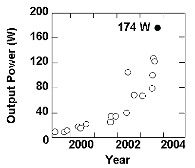 Power output of Fujitsu's newly developed GaN HEMT amplifier (Black circle indicates successful 63V operation, white circles indicate past results)
 -
[1] GaN
A type of wide band-gap semiconductor that is more resistant to breakdown at a given voltage than conventional semiconductors, such as gallium arsenide and silicon.
-
[2] HEMT
A field-effect transistor that takes advantage of operation of the electron layer at the boundary between different semiconductor materials that is relatively rapid compared to that within conventional semiconductors. Fujitsu led the industry with its development of HEMT technology in 1980, and the technology now underpins much of today's fundamental IT infrastructure, including satellite transceivers, wireless equipment, GPS-based navigation systems, and broadband wireless networking systems.
-
[3] distortion compensation circuits
Fujitsu's distortion compensation technology is based on the Digital Pre-Distortion (DPD) method, which adds compensatory characteristics to the signal before distortion occurs. Fujitsu has incorporated this technology into a distortion-compensation LSI.
-
[4] maximum power-added efficiency
A ratio indicating the conversion efficiency of direct current as an output signal supplied to an amplifier, converted to high-frequency power.
-
[5] W-CDMA
A 3G wireless standard, enabling flexible, high-speed data transmission. Also known as wide code-division multiple access, it permits multiplexed, distributed communications for multiple simultaneous users using spread encoding. Because multiple users can use the same frequency at the same time, this makes for an efficient use of spectrum. W-CDMA is one form of CDMA technology.
-
[6] adjacent channel leakage
A ratio that indicates the degree to which signals of adjacent channels are affected, due to amplifier distortion. As one of the critical specifications for amplifiers, the 3G system specification is much more stringent than that of the 2G base station.
-
[7] drain efficiency
A ratio indicating the conversion efficiency of direct current as an output signal supplied to an amplifier, converted to high-frequency power. For 3G base stations, output should not be at maximum power-added efficiency levels, but rather should be kept at an average power that satisfies the specification requirements for distortion (roughly 1/6th maximum power). The drain efficiency at this power level is an important specification for 3G base station amplifiers.
About Fujitsu Laboratories Ltd.
Founded in 1968 as wholly owned subsidiary of Fujitsu Limited, Fujitsu Laboratories Limited is one of the premier research centers in the world. With a global network of laboratories in Japan, China, the United States and Europe, the organization conducts a wide range of basic and applied research in the areas of Multimedia, Personal Systems, Networks, Peripherals, Advanced Materials and Electronic Devices.
For more information, please see: uk.fujitsu.com
Press Contacts
Public & Investor RelationsInquiries
Address: 1-5-2 Higashi-Shimbashi, Minato-ku, Tokyo Japan 105-7123
![]() Phone: +81 (0) 3-6252-2176
Phone: +81 (0) 3-6252-2176
Fax: +81 (0) 3-6252-2783
Company:Fujitsu Limited
Press Contacts
Photonics & Electronics Laboratories
![]() Phone: +81-46-250-8242
Phone: +81-46-250-8242
![]() E-mail: gan@ml.labs.fujitsu.com
E-mail: gan@ml.labs.fujitsu.com
Company:Fujitsu Laboratories Ltd.
All company/product names mentioned may be trademarks or registered trademarks of their respective holders and are used for identification purpose only.
Please understand that product prices, specifications and other details are current on the day of issue of the press release, however, may change thereafter without notice.
Date: 08 December, 2003
City: Kawasaki
Company:
Fujitsu Laboratories Ltd.,
,
,
,
,