![]()
Archived content
NOTE: this is an archived page and the content is likely to be out of date.
Fujitsu Develops World's First 12-Port, 10 Gbps Ethernet Switch on a Single Chip
Expected to lead to dramatic reductions in equipment size and cost
Fujitsu Limited,Fujitsu Laboratories Ltd.,Fujitsu Laboratories of America Inc.
Fujitsu Laboratories of America, Inc., working with Fujitsu Laboratories Ltd. and Fujitsu Limited, has succeeded in developing the world's first single chip implementation of a 12-port, 10 gigabits per second (Gbps) Ethernet switch.
The newly developed technology puts all the requirements for a 10 Gbps switch used to connect servers and storage devices on a single board in place of the bulky equipment that was previously required, thereby paving the way for dramatically more compact and less expensive systems overall.
Details on the new technology will be presented at Hot Chips 15, A Symposium on High-performance Chips, to be held in August in Palo Alto, California.
Background
There is a strong need for high-performance, standard interconnects that can be used for constructing flexible, reliable networks of high-speed servers and high-capacity storage systems. In particular, demand is expected to expand for super-fast Ethernet switches that operate at 10 Gbps and are compatible with the widely-used Internet Protocol.
Existing 10 Gbps switches, however, are bulky equipment designed for wide-area networks. Because of their large physical size, long switching latency and high cost, they have not been considered appropriate for cluster systems connecting blade servers or servers and storage units. Also, since they are not specifically designed for server-to-server or server-to-storage connections, supporting an extensive array of functions in a compact, low-cost unit posed various challenges. Fujitsu therefore decided to focus on functionality for server to storage interconnects, in order to develop technology for a single-chip implementation that would meet requirements for reduced size, price, and increased performance.
About the Technology
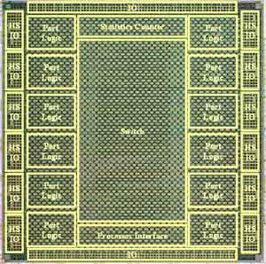
Some of the notable aspects of Fujitsu's new 10 Gbps Ethernet switch are as follows (see also Figure 1).
- 12-port, 10 Gbps switch integrated onto a single chip
By implementing layer-2 switching(1) as a basic function and newly developing the structure and control of the shared memory and crossbar, twelve 10 Gbps Ethernet ports, including the high-speed buffer memory required for switching and high-speed I/O macros, were condensed onto a single chip measuring 256 square millimeters. - High-performance switching core realizes high bandwidth of 240 Gbps Fujitsu's new Multi-port Stream Memory technology optimizes use of multiple memory blocks on the chip and their interconnections, giving the chip high-speed, high-capacity shared memory for multiple ports. This high-performance shared memory can handle both read and write operations simultaneously for all of the twelve 10 Gbps ports, providing a total bandwidth capacity of 240 Gbps.
- Newly developed memory control method dramatically reduces latency In order to pass an incoming packet to the output side in the least amount of time, Fujitsu developed a new scheduling control method for the shared memory. Whereas conventional switches have fall-through latency of several microseconds, the latency of Fujitsu's new switch is just 450 nanoseconds, or less than one-quarter the level of existing switches
Implementing the 10 Gbps Ethernet switch on a single chip required a LSI design technology that allowed intermixing of high-speed digital and analog circuits. This breakthrough was achieved by capitalizing on the collective strengths of Fujitsu Laboratories of America, Fujitsu Laboratories and Fujitsu Limited in high-speed I/O circuit design, chip integration, and packaging technologies.
The new 10 Gbps switch chip is slated to go into commercial production during 2003, and Fujitsu is now accelerating its development efforts toward advanced cluster systems, high-performance servers, and IP storage switches that could take advantage of this new technology. In addition, while 10 Gbps Ethernet transmission has to date required expensive optical modules, to enable more economical server construction, Fujitsu Laboratories of America has already developed an I/O circuit that can electrically transmit a 10 Gbps Ethernet signal over 20 meters. Work is underway to incorporate this I/O circuit into an enhanced version of this switch chip.
The development of this switch chip was partially funded by the New Energy and Industrial Technology Development Organization (NEDO), which is one of the Japanese Governmental Agencies.
-
[1] layer-2 switching
Switching using address information at the data-link layer (OSI network model).
About Fujitsu
Fujitsu is a leading provider of customer-focused IT and communications solutions for the global marketplace. Pace-setting technologies, highly reliable computing and telecommunications platforms, and a worldwide corps of systems and services experts uniquely position Fujitsu to deliver comprehensive solutions that open up infinite possibilities for its customers' success. Headquartered in Tokyo, Fujitsu Limited (TSE:6702) reported consolidated revenues of 4.6 trillion yen (US$38 billion) for the fiscal year ended March 31, 2003.
For more information, please see: www.fujitsu.com
About Fujitsu Laboratories of America, Inc.
Fujitsu Laboratories of America, Inc. is a wholly owned subsidiary of Fujitsu Laboratories Ltd. (Japan), focusing on research on advanced VLSI CAD, Internet, and interconnect technologies. Conducting research in an open environment, it contributes to the global research community and the working IT industry. It is headquartered in Sunnyvale, CA.
For more information, please see: www.fla.fujitsu.com
About Fujitsu Laboratories Ltd.
Founded in 1968 as a wholly owned subsidiary of Fujitsu Limited, Fujitsu Laboratories Limited is one of the premier research centers in the world. With a global network of laboratories in Japan, China, the United States and Europe, the organization conducts a wide range of basic and applied research in the areas of Multimedia, Personal Systems, Networks, Peripherals, Advanced Materials and Electronic Devices.
For more information, please see: www.fla.fujitsu.com
Press Contacts
Public & Investor RelationsAddress: 1-5-2 Higashi-Shimbashi, Minato-ku, Tokyo Japan 105-7123
![]() Phone: +81-3-6252-2176
Phone: +81-3-6252-2176
Fax: +81 (0) 3-6252-2783
Company:Fujitsu Limited
Technical Contacts
Advanced Interconnect Technology Dept
![]() Phone: +1-408-530-4577
Phone: +1-408-530-4577
![]() E-mail: hattori@fla.fujitsu.com
E-mail: hattori@fla.fujitsu.com
Company:Fujitsu Laboratories of America, Inc
Technical Contacts
IT Architecture Laboratory, IT Core Laboratories
![]() Phone: +81-44-754-2665
Phone: +81-44-754-2665
![]() E-mail: xgchip@ml.labs.fujitsu.com
E-mail: xgchip@ml.labs.fujitsu.com
Company:Fujitsu Laboratories Ltd.
All company/product names mentioned may be trademarks or registered trademarks of their respective holders and are used for identification purpose only.
Please understand that product prices, specifications and other details are current on the day of issue of the press release, however, may change thereafter without notice.
Press Release ID: 2003-0093
Date: 14 May, 2003
City: Tokyo
Company:
Fujitsu Limited,
Fujitsu Laboratories Ltd.,
Fujitsu Laboratories of America, Inc.,
,
,