Kawasaki, Japan, March 21, 2013
Fujitsu Laboratories Limited announced the development of a four-wavelength integrated silicon laser for optical transceivers(1) that use silicon photonics(2), a step toward faster data communications between processors.
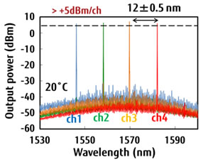
One effective way to increase the capacity of data transfers is to carry multiple signals, each at a different wavelength, over the same optical fiber (multiplexing). Typically, in silicon photonics there would be different sized ring resonators(3) to generate optical signals for each wavelength. However, maintaining precise spacing between each wavelength is problematic due to variations in manufacturing processes as well as temperature fluctuations. Also, high-power signals are needed to compensate for losses that occur when multiplexing and demultiplexing signals. Fujitsu Laboratories has succeeded in making use of the periodic transparency of ring resonators to generate wide and uniform wavelength spacing of laser light. Also, mounting technologies that precisely connect multiple silicon waveguides and optical amplifiers on the silicon reduce connection loss between waveguides and achieves a higher power output. The resulting integrated silicon laser has been proven to generate four wavelengths consistently with a wide spacing of 12±0.5 nm and high output of +5 dBm.
This technology helps pave the way toward faster inter-processor communications, which will be a key element in future high-performance computers, such as exaflops-class(4) supercomputers and high-end servers.
Details of this technology are being presented at the Optical Fiber Communication Conference and Exposition and the National Fiber Optic Engineers Conference (OFC/NFOEC 2013), running March 17-21 in Anaheim, California.
Background
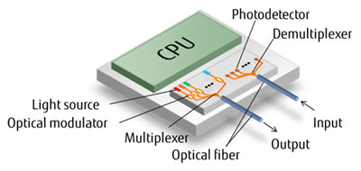
In recent years, the processing speed of supercomputers and high-end servers has been roughly doubling every 18 months. At this pace, by around 2018, high-capacity data-transfer technologies will need to support data input/output speeds of several terabits per second. As a result, consideration is being given to the use of optical interconnect technology in which processors are connected using light (figure 1). Recently, in particular, attention is being focused on the development of silicon photonics technology enabling optical transceivers to that are compact, yet suitable for LSI applications, thereby facilitating integration of electrical and optical components.
 Figure 1: Integrated silicon optical transceiver for large-volume data transmission
Technological Issues
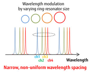
Multiplexing, in which multiple optical signals, each at a different wavelength, are joined and carried over the same optical fiber, is an effective method for high-volume data transfers between processors. For this reason, wave-division multiplexing technology has been adapted to silicon photonics as well. This has typically been done using a separate ring resonator, each with a different size, to generate each wavelength (channels 1–4). The circumference of each ring resonator determines the wavelength it generates, but variations in manufacturing processes often lead to the problem of wavelengths with non-uniform spacing (Figure 2). When the spacing between wavelengths winds up being close, temperature variations can cause additional wavelength shifts so that individual wavelengths become difficult to distinguish. Furthermore, temperature-adjustment circuits for each wavelength, which compensate for these temperature-induced wavelength shifts, increase device complexity. In addition to generating wavelengths at a very precise level, the signals need to have a high power output to compensate for losses that occur when multiplexing and demultiplexing them.
 Figure 2: Issues with wavelength-division multiplexing using existing silicon photonics methods
Newly Developed Technology
Fujitsu Laboratories has found a way to generate consistent wavelengths over a wide range by using the periodic transparency inherent in ring resonators. It has also developed a mounting technology that creates high-precision connections between multiple silicon waveguides and optical amplifiers, which reduces connection loss. This results in an integrated silicon laser that generates four consistent wavelengths with a wide spacing of 12±0.5 nm, and high power output of +5 dBm. The features of the technology are as follows.
1. Laser-oscillator wavelength-control technology
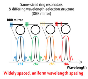
This technology generates widely spaced, yet consistent signals at multiple, different wavelengths. Each laser consists of four identically sized ring resonators (Figure 3), which act as wavelength filters, having periodic transparency. Each ring resonator is also equipped with a wavelength-selection mechanism (a DBR mirror(5)) that selects one of the periodic wavelengths, so that four distinct wavelengths can be generated.
 Figure 3: Concept behind newly developed on-chip, integrated 4-wavelength laser
In this configuration, each ring resonator has the same size and the same periodic characteristics, so the spacing between wavelengths is determined by the periodic characteristics of the ring resonators, rather than the ring-resonator circumference, as had been the case with previous technologies. This means that each laser can be generated at a precise, uniformly spaced wavelength. Furthermore, combining this configuration with modulators that use same-sized ring resonators cancels out the wavelength shifts that accompany temperature fluctuations. This construction allows for an optical transmitter that does not require a temperature-control circuit, which would otherwise consume a significant amount of electricity, even in environments with changing temperatures, such as a processor package.
2. Technology for low-loss amplifier couplings
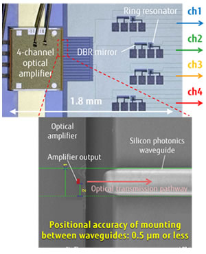
This is a high-precision mounting technology for placing optical amplifiers on the silicon substrate. Applying the optical amplifier directly to the silicon waveguide with a margin of error within ±0.5 µm reduces connection losses between the optical amplifier and silicon resonator, and results in an integrated silicon laser with +5 dBm of output power, sufficient for wavelength-division multiplexing (Figure 5).
 Figure 4: Prototype 4-wavelength integrated silicon laser
 Figure 5: Characteristics of the prototype 4-wavelength integrated silicon laser
Results
By using this technology to integrate multiple optical transmitters on a single chip, it will be possible to create optical transmitters small enough to be embedded into CPU modules capable of transmitting large volumes of data at rates of several terabits per second. This is a step towards future high-performance computers, such as exaflops-class supercomputers and high-end servers, which will demand high-capacity data transfers between CPUs.
Future Plans
Fujitsu Laboratories is developing an optical receiver compatible with wavelength-division multiplexing that uses silicon photonics, and by integrating that with the newly developed optical transmitter, plans to produce a compact optical transceiver. Furthermore, the company is continuing to work on advances in LSI and mounting technology, and is developing compact, integrated interconnects that can be included in CPU packages for terabit-class data transfers.
![]() E-mail: si-photonics-3@ml.labs.fujitsu.com
E-mail: si-photonics-3@ml.labs.fujitsu.com