![]()
Archived content
NOTE: this is an archived page and the content is likely to be out of date.
Fujitsu Develops Compact, High-Performance and Energy-Efficient DSP for Mobile Device Baseband Processing
Leverages supercomputer technology to lower energy requirements for smartphones and other wireless mobile devices
Fujitsu Laboratories Ltd.
Fujitsu Laboratories Limited today announced the development of a digital signal processor (DSP) for use in mobile device baseband processing. By employing a vector processing architecture(1) as used in supercomputers, the DSP can efficiently run highly repetitive processes common in LTE(2) and other wireless processes. This, in turn, allows for greater energy efficiency.
By using 28-nanometer (nm) process technology and when running at 250 MHz, DSP is capable of processing data at 12 GOPS (12 billion operations per second). Excluding memory, the DSP measures only 0.4 mm2, and it consumes only 30 milliwatts (mW) of power, 20% less than existing DSPs.
The new DSP is expected to help lengthen talk times, usage times and standby times for smartphones and other mobile devices. In addition, revisions to the signal processing algorithm can be implemented through modifications to the DSP program, enabling fine-tuning of reception characteristics after the wireless baseband LSI has been manufactured, thereby contributing to shorter development lead times.
Details of the new technology will be presented at the 2013 International Symposium on VLSI Design, Automation and Test (2013 VLSI-DAT), scheduled to open on April 22 in Taiwan.
Background
In recent years, smartphones, tablets, and other wireless devices have rapidly gained in popularity. As the speed of wireless networks increase, manufacturers have launched models that support new wireless communications standards such as LTE, which is currently being rolled out worldwide, in addition to conventional standards such as GSM and 3G. To support these wireless standards, a signal processing circuit (baseband processor) compliant with each computation is required. As a result, being able to reduce the size and power consumption of baseband processor components is crucial to improving the cost and battery life of devices.
Technological Challenges
Typical baseband processing circuits are implemented using specialized hardware to support each communications standard, requiring a number of circuits to support different standards. Consequently, reducing the size of circuits has proved challenging. On the other hand, there exist alternative software-based approaches to supporting each communications standards using DSPs. Given the massive signal processing requirements of LTE, however, these approaches are limited in their ability to simultaneously achieve both high processing performance and low energy consumption.
Newly Developed Technology
Fujitsu Laboratories has developed a new DSP that employs a vector processing architecture used in supercomputers. The DSP can efficiently run highly repetitive processes that are common in LTE and other wireless processes, thereby achieving greater energy efficiency.
Key features of the newly developed DSP are as follows:
1) Vector processing architecture
The DSP employs a vector architecture found in supercomputers. With a typical processor, a single instruction will be executed on a single piece of data at a time (scalar data). By contrast, a vector processor will execute a single instruction on multiple pieces of data (vector data) at a time. As a result, when repeating the same process for multiple data elements, the ability of the vector architecture to complete a task with a single instruction makes it possible to cut down on the amount of processing and energy required to read and decode instructions from the memory.
LTE uses the OFDM(3) modulation method and communicates by bundling data that is carried by up to 1,200 "subcarriers" in a wireless signal. To extract information from an incoming signal, the DSP must apply the same process repeatedly for each subcarrier. This makes the vector approach more effective.
Figure 1 shows a block diagram of the newly developed DSP. The DSP consists of a vector engine, which employs a vector architecture, as well as a conventional CPU. The CPU reads in program code from the instruction memory, decodes the instruction, and if the vector approach is suitable for use on the instruction, it is transferred to the vector engine where it is executed. Other instructions are executed in the CPU as usual.
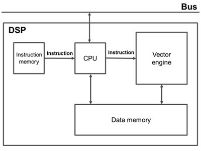 Figure 1: DSP block diagram
2) Vector engine optimized for baseband processing
Figure 2 shows an internal diagram of the vector engine itself. Instructions transferred from the CPU are stored in the instruction buffer. Stored instructions are decoded one by one by the sequencer, and the required vector processing pipeline(4) is controlled to execute the instruction. The number of vector data (vector length) that can be calculated in a single instruction is 64 data elements, a value optimized for use in mobile device baseband processing. Rather than processing 64 data elements sequentially, eight parallel processing elements process the data in eight rounds, thereby achieving higher speeds.
The vector engine features a small circuit size, and to increase the efficiency of baseband processing, there are two pipelines for processing multiply instructions on vector data, and there are also two pipelines for processing load instructions (or conversely, store instructions) that load vector data to the register file, which temporarily stores data from memory, for a total of four pipelines. All four pipelines can process addition, subtraction, and logic operations on vector data.
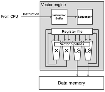 Figure 2: Vector engine block diagram
Results
With the addition of the newly developed vector engine, many pieces of data can be processed with a single instruction, thereby enabling more efficient data processing. This, in turn, will significantly contribute to reduced energy consumption in wireless baseband LSIs. A DSP using 28nm process technology and running at 250 MHz is able to process 12 GOPS (12 billion operations per second). Fujitsu Laboratories succeeded in developing a compact DSP that measures only 0.4 mm2 (without memory) and, in terms of power consumption, requires only 30mW—a 20% improvement over existing DSPs.
The new DSP is expected to help lengthen talk times, usage times and standby times for smartphones and other mobile phones. In addition, revisions to the signal processing algorithm can be implemented through modifications to the DSP program, enabling fine-tuning of reception characteristics after the wireless baseband LSI has been manufactured, thereby contributing to shorter development lead times.
Future Development
The new DSP will be incorporated into a communications processor from Access Network Technology Limited that is scheduled for use in Fujitsu smartphones and elsewhere. Going forward, Fujitsu Laboratories plans to continue making performance improvements to the processor to enable it to keep pace with advances in higher speed wireless communications standards.
-
[1] Vector processing architecture
A processor architecture for processing calculations on vector data (a one-dimensional array of data) with a single instruction.
-
[2] Long Term Evolution (LTE)
The name of the latest mobile communications standard for wireless devices.
-
[3] Orthogonal Frequency-Division Multiplexing (OFDM)
A wireless modulation encoding used also in wireless LANs.
-
[4] Processing pipeline
A circuit that executes an arithmetic process according to an instruction. By dividing execution into multiple stages, the calculation is executed according to a workflow process.
About Fujitsu
Fujitsu is the leading Japanese information and communication technology (ICT) company offering a full range of technology products, solutions and services. Over 170,000 Fujitsu people support customers in more than 100 countries. We use our experience and the power of ICT to shape the future of society with our customers. Fujitsu Limited (TSE:6702) reported consolidated revenues of 4.5 trillion yen (US$54 billion) for the fiscal year ended March 31, 2012. For more information, please see http://www.fujitsu.com.
About Fujitsu Laboratories
Founded in 1968 as a wholly owned subsidiary of Fujitsu Limited, Fujitsu Laboratories Limited is one of the premier research centers in the world. With a global network of laboratories in Japan, China, the United States and Europe, the organization conducts a wide range of basic and applied research in the areas of Next-generation Services, Computer Servers, Networks, Electronic Devices and Advanced Materials. For more information, please see: http://jp.fujitsu.com/labs/en.
Technical Contacts
Platform Technologies LaboratoriesProcessor Solution Development Lab.
![]() E-mail: psdl_vu@ml.labs.fujitsu.com
E-mail: psdl_vu@ml.labs.fujitsu.com
Company:Fujitsu Laboratories Ltd.
All company or product names mentioned herein are trademarks or registered trademarks of their respective owners. Information provided in this press release is accurate at time of publication and is subject to change without advance notice.
This press release has been revised as of December 17, 2018.
Date: 01 February, 2013
City: Kawasaki, Japan
Company:
Fujitsu Laboratories Ltd.,
,
,
,
,
,
,
,
,
,