![]()
Archived content
NOTE: this is an archived page and the content is likely to be out of date.
Fujitsu Develops World's First Compact, High-Output, Single-Chip 10 GHz Transceiver Using GaN HEMT
Reduces chip footprint by over 90%, enabling more compact radars and wireless communications equipment
Fujitsu Laboratories Ltd.
Fujitsu Laboratories today announced that it has successfully developed the world's first single-chip transceiver using gallium nitride (GaN)(1)high electron mobility transistor (HEMT)(2) technology that features an output of 6.3 W and that operates at a frequency of 10 GHz.
In order to simultaneously handle strong transmission signals and weak incoming signals in the same chip, it is necessary to efficiently switch between outgoing and incoming signals, while reducing the impact that outgoing signals have on incoming signals. However, until now, it has been technologically difficult to accomplish both of these objectives in tandem.
Fujitsu Laboratories has resolved this issue by developing a duplexer with low signal loss using a GaN-HEMT, and through high-output circuit integration design technology that controls signal interference between the outgoing and incoming signals. The result is a transceiver chip operating at a frequency of 10 GHz with output of 6.3 W that measures only 3.6mm x 3.3mm, representing a footprint that is less than 10% of the size of the multiple chips that have been needed until now.
With this technology, it is now possible to configure a high-output transceiver using just one chip, enabling systems such as radar equipment and wireless communications equipment to be made more compact.
Details of this technology were presented at the IEEE MTT International Microwave Symposium (IMS 2012) held in Montreal starting June 17.
GaN HEMT
Gallium nitride (GaN) is used as a material in blue LEDs. Compared to the conventional semiconductor materials of silicon (Si) and gallium arsenide (GaAs), GaN features a high electron transfer rate and relative resistance to the breakdown caused by voltage. Given these characteristics, GaN HEMTs—or transistors that use GaN—show promise for high-output, exceptionally efficient operations.
Background
In line with the advancement of a network-based society, radio wave demand in a variety of wireless systems is expected to increase even further. For example, aircraft radar uses the 10 GHz frequency band, which is able to measure the distance and direction of physical objects with high precision.
Existing radars are configured with separate equipment for transmitters and receivers. A transceiver chip that integrates both functions, however, would enable everything to be integrated in one piece of equipment, allowing systems to become more compact.
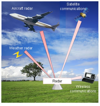 Figure 1: Typical uses of the 10-GHz band
Technical Issues
The transceiver chips necessary to make radar and other equipment more compact must deliver high-capacity communications and high output in order to cover a large area. Transmitting high-power signals using the same chip that receives low-power signals requires high-efficiency switching in the outbound signal and reduced impact of outbound signals on inbound signals. Achieving both of these goals has been problematic.
Newly Developed Technology
Fujitsu Laboratories developed the world's first single, compact transceiver chip that uses GaN-HEMT and operates in the 10-GHz band. Its key features are as follows:
1. Ultra-compact transmit/receive switch
A new duplexer was developed that uses GaN-HEMT (Figure 2, right). This measures 1.8 mm × 2.4 mm, with 1.1 dB transmission loss in the 0–12 GHz range. This is dramatically smaller and lighter than earlier switches using magnetic materials (Figure 2, left)—less than 10% the size.
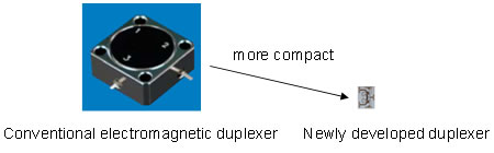 Figure 2: Comparison of conventional transmit/receive switches and the newly developed one
2. High-output circuit integration design technology
Via holes for grounding are arrayed around the transistors, shielding against the release of unwanted signals. In addition, the locations and layouts of signal wiring and circuitry were optimized using three-dimensional analysis of electromagnetic radiation to suppress unwanted signal interference (Figure 3). This technology ensures stable operation, preventing the oscillations of high-power circuitry from causing malfunctions.
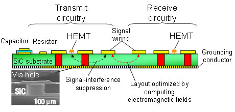 Figure 3: Technologies to suppress unwanted signal interference
These technologies were integrated into a single prototype chip that combines a duplexer, a transmitting amplifier, and a receiving amplifier (Figure 4). The chip operates at 6.3 W in the 10-GHz band and measures 3.6 × 3.3 mm, less than one-tenth the size of earlier multi-chip systems.
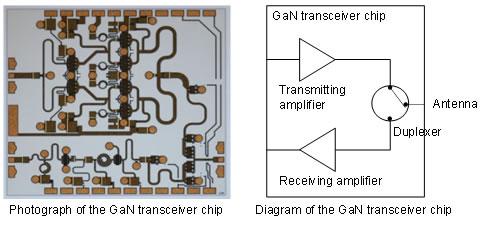 Figure 4: Photo and diagram of the newly developed GaN transceiver chip
Results
These technologies make it possible to design a high-output transceiver around a single chip, with applications in radar and broadband communications, promising smaller, lighter systems.
Future Plans
Fujitsu Laboratories intends for this technology to be put to use in a wide range of applications that require compact modules with high output, including wireless communications and radar systems.
-
[1] Gallium nitride (GaN)
GaN-based semiconductors are wide bandgap semiconductors that feature a higher breakdown-voltage (threshold) than conventional semiconductor materials, such as silicon (Si) or gallium arsenide (GaAs).
-
[2] High electron mobility transistor (HEMT)
A field-effect transistor that utilizes the electron movement at the junction between two semiconductors with different bandgaps—as electron mobility in HEMTs is faster than that of conventional semiconductors. Fujitsu led the industry with its development of HEMT technology in 1980, and HEMTs, as a core technology underpinning the network-based society, are currently used in a wide range of core technologies for IT applications, including satellite transceivers, mobile phones, GPS-based navigations systems, and broadband wireless networking systems.
About Fujitsu
Fujitsu is the leading Japanese information and communication technology (ICT) company offering a full range of technology products, solutions and services. Over 170,000 Fujitsu people support customers in more than 100 countries. We use our experience and the power of ICT to shape the future of society with our customers. Fujitsu Limited (TSE:6702) reported consolidated revenues of 4.5 trillion yen (US$54 billion) for the fiscal year ended March 31, 2012. For more information, please see http://www.fujitsu.com.
About Fujitsu Laboratories
Founded in 1968 as a wholly owned subsidiary of Fujitsu Limited, Fujitsu Laboratories Limited is one of the premier research centers in the world. With a global network of laboratories in Japan, China, the United States and Europe, the organization conducts a wide range of basic and applied research in the areas of Next-generation Services, Computer Servers, Networks, Electronic Devices and Advanced Materials. For more information, please see: http://jp.fujitsu.com/labs/en.
Technical Contacts
Devices & Materials LaboratoriesAdvanced Devices Lab.
![]() E-mail: gan-hemt-press@ml.labs.fujitsu.com
E-mail: gan-hemt-press@ml.labs.fujitsu.com
Company:Fujitsu Laboratories Ltd.
All other company or product names mentioned herein are trademarks or registered trademarks of their respective owners. Information provided in this press release is accurate at time of publication and is subject to change without advance notice.
Date: 20 June, 2012
City: Kawasaki, Japan
Company:
Fujitsu Laboratories Ltd.,
,
,
,
,
,
,
,
,
,