![]()
Archived content
NOTE: this is an archived page and the content is likely to be out of date.
Fujitsu Develops CMOS Logic-Based High-Voltage Transistor for Power Amplifiers
- Enables single-chip integration of power amplifiers and CMOS logic control circuitry -
Fujitsu Laboratories Ltd.,Fujitsu Microelectronics
Fujitsu Laboratories Limited and Fujitsu Microelectronics Limited today announced the development of a CMOS logic(1) process-based high-voltage transistor featuring high breakdown voltage, suitable for power amplifiers used in wireless devices. As a world's first, Fujitsu developed a 45 nanometer (45nm)-generation CMOS-based transistor capable of handling 10 V power output, thus enabling the transistor to handle high-output requirements necessary for power amplifiers used in WiMAX(2) and other high-frequency applications. The new technology makes it possible for power amplifiers to be formed on the same die as CMOS logic control circuitry to achieve single-chip integration, thereby making high-performance, low-cost power amplifiers feasible.
Details of this technology were presented at the 2008 IEEE International Electron Devices Meeting (IEDM) held from December 15 to 17 in San Francisco. (Session/Presentation: 19.1)
Background
Due to the fact that power amplifiers for wireless devices demand high power output at high frequencies, currently compound semiconductors such as gallium-arsenide (GaAs) are commonly used, mounted as a chip separate from control circuitry based on a general-purpose CMOS logic chip. If these chips' functions could be integrated onto a single chip, it would enable cost reduction of the overall module and likely speed adoption of wireless devices to be used with wireless communication standards such as WiMAX and LTE(3). Thus, there is a need for transistors that are compatible with CMOS logic process technology, and which can satisfy the requirements of power amplifiers necessary for WiMAX and other wireless communication standards.
Technological Challenges
The power output required of power amplifiers for use in high-frequency applications, such as WiMAX, exceeds the breakdown voltage of transistors used with standard CMOS logic processes. Overcoming this hurdle while remaining compatible with CMOS process technology requires an increase in the transistor's breakdown voltage, which is achieved with a structure that lowers the electric field around the drain, as electric fields can lead to transistor failure. Furthermore, structures with high breakdown voltages typically increase the transistor's on-resistance(4), making it difficult to obtain satisfactory performance at high frequencies. Therefore, any solution would need to both raise breakdown voltage and avoid increasing on-resistance.
Newly Developed Technology
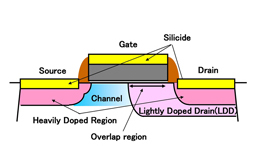 Figure 1: Structure of Fujitsu's newly developed transistor
Larger View (146 KB)
To overcome the aforementioned issues, Fujitsu developed a new transistor structure with the following key characteristics (Figure 1):
- The transistor's drain is surrounded by a "lightly doped drain" (LDD) region, which overlaps with the gate. This lowers the electrical field extending horizontally to the drain, and the electrical field extending to the gate oxide layer, thereby raising the breakdown voltage.
- The dopant distribution in the transistor channel follows a lateral gradient. This lowers the density of dopant on the drain side of the channel, thus limiting the increase in drain resistance, which is the main part of on-resistance. It also lowers the electrical field extending horizontally to the drain, also raising the breakdown voltage.
The typical method for raising the breakdown voltage of a CMOS transistor has been to widen the gap separating gate and drain. This new structure suppresses on-resistance effectively compared to the conventional method, without increasing the gap.
Furthermore, this new structure is believed to be highly compatible with standard transistors with 3.3 V I/O(5), since it requires only the additional steps of forming the LDD region and the custom channel region.
Results
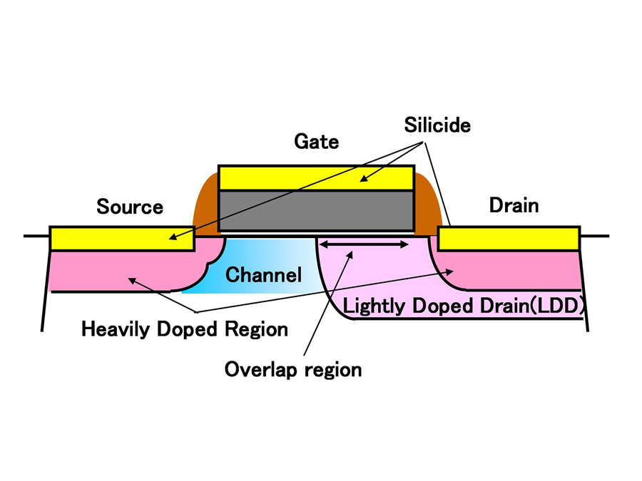
 Figure 2: Characteristics of Fujitsu's new power-transistor(measured frequency: 2.1GHz; gate width: 0.32mm)
Larger View (176 KB)
By using 45nm process technology to apply the new transistor's technology to standard transistors with 3.3 V I/O, Fujitsu developed the world's first transistor that raises the breakdown voltage from 6 V to 10 V. In regard to features that make the new transistor suitable for use in power amplifiers, power output of 0.6 W per gate width of 1mm (0.6 W/mm) was reached at maximum oscillation frequency of 43 GHz (Figure 2), thereby demonstrating sufficient performance for use as a power transistor in WiMAX. The new transistor also produced good results in basic reliability testing.
Future Developments
Fujitsu's newly developed high-voltage transistor paves the way for CMOS logic-based transistors featuring high breakdown voltages for use in power amplifiers. Fujitsu will continue with further advances for this technology, striving for single-chip integration of power amplifiers and control circuitry, to realize low-cost high-performance power amplifier modules.
For more information:
-
[1] CMOS logic
A logic circuit consisting of N-type (negative-type) and P-type (positive-type) metal-oxide semiconductor (MOS) transistors with complementary interconnects. Complementary metal-oxide semiconductor (CMOS) logic chips are currently the mainstream for integrated circuits, attributable to their low power consumption.
-
[2] WiMAX
Worldwide Interoperability for Microwave Access. A standard for wireless communications that is anticipated to become widespread in the future for wireless devices.
-
[3] LTE
Long Term Evolution. A new mobile phone communications standard, for which services are expected to start from around 2010.
-
[4] On-resistance
Resistance between the source and drain when a transistor is on. The lower the on-resistance, the higher the efficiency and the better the high-output characteristics.
-
[5] I/O transistor
Transistor in the I/O circuit, embedded in an integrated circuit (IC), that handles the exchange of signals with external components. In many cases, the I/O circuitry operates at a higher voltage than the IC's internal parts, with 3.3 V I/O transistors being one of the most common.
About Fujitsu Laboratories
Founded in 1968 as a wholly owned subsidiary of Fujitsu Limited, Fujitsu Laboratories Limited is one of the premier research centers in the world. With a global network of laboratories in Japan, China, the United States and Europe, the organization conducts a wide range of basic and applied research in the areas of Multimedia, Personal Systems, Networks, Peripherals, Advanced Materials and Electronic Devices. For more information, please see:http://jp.fujitsu.com/group/labs/en/
About Fujitsu Microelectronics (FML)
Fujitsu Microelectronics Limited (FML) is a large-scale integrated circuit (LSI) manufacturer that provides highly reliable, optimal solutions to meet the varying needs of its customers, through LSI offerings including ASIC/COT, ASSP and power management ICs, and flash microcontrollers. Along with building on its wide-range expertise focusing on imaging, wireless, and security LSI applications, FML also pursues initiatives for power efficiency and undertakes environmentally-conscious countermeasures. Headquartered in Tokyo, FML was established as a subsidiary of Fujitsu Limited on March 21, 2008. Through its global sales and development network with sites in Japan and other regions in Asia, Europe, and the U.S., FML offers LSI solutions to the global marketplace. For more information:http://jp.fujitsu.com/group/fml/en/
Technical Contacts
Technology Development DivisionCommon IP & Technology Development Unit
![]() Phone: +81(42)532-1488
Phone: +81(42)532-1488
![]() E-mail: cmos-pa@ml.labs.fujitsu.com
E-mail: cmos-pa@ml.labs.fujitsu.com
Company:Fujitsu Microelectronics Limited
Company and product names referenced herein are trademarks or registered trademarks of their respective owners. Information provided in this press release is accurate at time of publication and is subject to change without advance notice.
Date: 17 December, 2008
City: Kawasaki and Tokyo, Japan
Company:
Fujitsu Laboratories Ltd.,
Fujitsu Microelectronics Limited,
,
,
,