![]()
Archived content
NOTE: this is an archived page and the content is likely to be out of date.
Fujitsu Laboratories Develops Power Gating Technology to Enable Power Savings in System LSIs
- Permits rapid on/off power switching in less than one microsecond, an industry first -
Fujitsu Laboratories Ltd.,Fujitsu Microelectronics
Fujitsu Laboratories Limited and Fujitsu Microelectronics Limited announced today, as an industry first, the development of circuit technology that can rapidly switch a power supply from off to on in less than one microsecond. This makes it possible to extend the "off" period - sleep time - of a chip as a means to reduce leakage current, enabling highly integrated LSI chips to consume less power. Details of this technology will be presented at the 2008 Symposium on VLSI Circuits, to be held from June 18 to June 20 in Honolulu, Hawaii.
Background
As LSIs become more highly integrated, their leakage current(1) increases. Mobile phones in particular, which may be idling for long periods of time with the power supply on but the processing circuitry being inactive, are especially susceptible to leakage current, thus increasing their power consumption and reducing their battery life. A technology called power gating can be used to switch off unused circuitry, but with existing power-gating techniques, switching from off to on takes several microseconds thus resulting in relatively long restoration times. The longer the restoration time, the shorter the sleep time and the less that leakage current has been suppressed. Furthermore, because the circuitry cannot be used during restoration, system performance is also degraded.
The goal for next-generation mobile devices has been to reduce this restoration time to one microsecond or less, but that had been impossible with existing power-gating techniques.
Technological Challenges
Recovering to the powered-on state requires the circuit to be recharged. With existing technologies, the current that flows in to charge the circuit - the rush current - is controlled by a weak switch, and once the circuit has been charged, a strong switch with the regular current supply quickly cuts in. To date, the focus has been on speeding up this overall process, but in order to achieve a faster restoration in this way, the rush current needs to be increased and thus caused considerable power supply noise(2). Since the power supply noise has an adverse effect on the circuits in operation, the rush current must be limited to a few millivolts. With existing techniques, bringing restoration time down to within one microsecond has required a lower power-supply impedance(3), which is impractical in real-world LSI applications because of greatly increased costs.
Newly Developed Technology
Thanks to advancements in existing power-gating technology by Fujitsu Microelectronics, this new technology is capable of rapid restoration times, with little power supply noise caused by rush current.
This new technology involves employing a dedicated bypass power line and connecting the weak switch - which is typically used to control the rush current - to this line only, and optimizing the sequence of switch operations. Thanks to this technique, the dedicated-bypass power-supply noise from the rush current cannot make its way through to the rest of the circuitry that is in operation and being powered by the primary power supply. As a result, the power-supply noise over the power line when rush current is on is cut to less than one-fourth, without lowering the impedance of the power supply. Even with the same power-supply noise, restoration time takes less than one-fourth as long as before.
Results
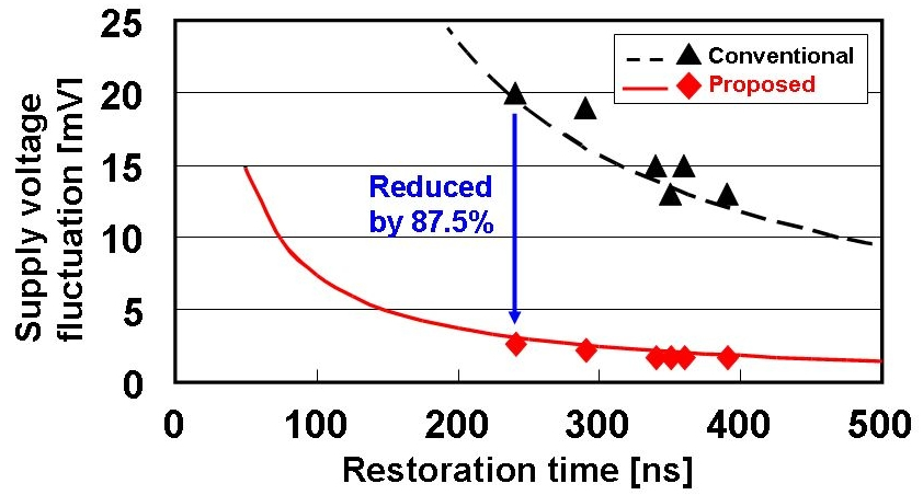
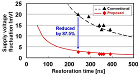 Figure 1: Evaluation test results using a finished product chip
Larger View (139 KB)
Fujitsu tested this technology on a dual-core processor with two million gates, manufactured using 90-nm process technology. The resulting restoration time was 240 nanoseconds and power-supply noise was 2.5 millivolts, compared to 20 millivolts for existing technologies, a reduction of 87.5% (see Figure 1). It was thus demonstrated that power restoration time could be reduced to under one microsecond, a result that would have been difficult to achieve with conventional technology.
Furthermore, the addition of the dedicated bypass power line increased chip area requirements by just less than 1%, having a trivial impact on overall chip space requirements.
Future Developments
Fujitsu Microelectronics plans to make this technology a core feature of its CoolAdjust™(4) systematic power-saving technology, adapting it to standard LSI design flows for 65nm and 45nm CMOS technologies, for ASSP(5) and ASIC(6) applications.
-
[1] Leakage current
Wasted current that is leaked when a circuit is idle.
-
[2] Power supply noise
Voltage fluctuations in a power supply that exert a negative influence over a LSI's internal circuit operations.
-
[3] Power-supply impedance
PA measure of the difficulty with which current flows, when supplied to a powered network. The unit of impedance is the ohm (Ω).
-
[4] CoolAdjust™
Fujitsu Microelectronics' power-saving technology that is based on power supply control. Comprised of power gating and technologies that optimize the body bias voltage and power-supply voltage, in response to process and thermal fluctuations.
-
[5] ASSP
Application-specific standard product. A general-purpose LSI featuring functions for specific applications.
-
[6] ASIC
Application-specific integrated circuit. A customized LSI for a specific purpose.
About Fujitsu Laboratories
Founded in 1968 as a wholly owned subsidiary of Fujitsu Limited, Fujitsu Laboratories Limited is one of the premier research centers in the world. With a global network of laboratories in Japan, China, the United States and Europe, the organization conducts a wide range of basic and applied research in the areas of Multimedia, Personal Systems, Networks, Peripherals, Advanced Materials and Electronic Devices. For more information, please see:http://jp.fujitsu.com/group/labs/en/
About Fujitsu Microelectronics (FML)
Fujitsu Microelectronics Limited (FML) is a large-scale integrated circuit (LSI) manufacturer that provides highly reliable, optimal solutions to meet the varying needs of its customers, through LSI offerings including ASIC/COT, ASSP and power management ICs, and flash microcontrollers. Along with building on its wide-range expertise focusing on imaging, wireless, and security LSI applications, FML also pursues initiatives for power efficiency and undertakes environmentally-conscious countermeasures. Headquartered in Tokyo, FML was established as a subsidiary of Fujitsu Limited on March 21, 2008. Through its global sales and development network with sites in Japan and other regions in Asia, Europe, and the U.S., FML offers LSI solutions to the global marketplace. For more information:http://jp.fujitsu.com/group/fml/en/
Technical Contacts
System LSI Development Lab.SOC Design Methodology Research Lab.
![]() Phone: +81-44-754-2657
Phone: +81-44-754-2657
![]() E-mail: lp-pg@ml.labs.fujitsu.com
E-mail: lp-pg@ml.labs.fujitsu.com
Company:Fujitsu Laboratories Limited
Company and product names referenced herein are trademarks or registered trademarks of their respective owners. Information provided in this press release is accurate at time of publication and is subject to change without advance notice.
Date: 17 June, 2008
City: Kawasaki and Tokyo, Japan
Company:
Fujitsu Laboratories Ltd.,
Fujitsu Microelectronics Ltd.,
,
,
,