![]()
Archived content
NOTE: this is an archived page and the content is likely to be out of date.
Fujitsu Succeeds in World's First Operation of 100W-Class Amplifiers Employing Carbon Nanotubes for Next-Generation Mobile Base Stations
- Major step closer toward practical use of 4G mobile communication systems -
Fujitsu Laboratories Ltd.
Fujitsu Laboratories Ltd. today announced that, using carbon nanotubes(1) as heat-dissipation material in amplifier transistors, Fujitsu has become the first to achieve the successful operation of high-frequency, high-power (100W-class) flip-chip(2) amplifiers employing carbon nanotubes, for mobile base stations designed for fourth-generation (4G, IMT-Advanced) systems. Fujitsu achieved high frequency, high output, and high amplification in the amplifiers by developing "dual-side heat-dissipation" technology, in which heat is dissipated through both sides of the transistor chip, which is the source of the amplifier's heat output. Furthermore, Fujitsu's new technology enables the reduction of the transistor chip size to less than two-thirds (2/3) the size of existing transistor chips. Details of this new technology were presented at the IEEE International Symposium on Radio-Frequency Integration Technology 2009 (RFIT 2009) held from December 9 to 11 in Singapore, at which Fujitsu Laboratories was awarded the RFIT 2009 Best Paper for Oral Presentation award.
Background
As a result of improvements in communication transmission speeds and mobile phone performance, the volume of data transmitted by mobile communications is dramatically increasing. It is envisioned that future 4G (IMT-Advanced) mobile communications systems will enable ultra-fast high-volume data transmissions of 50Mbps to 1Gbps, by utilizing wide bandwidths at high frequencies.
Accordingly, for wireless base stations that will serve to link mobile phones and data, there is demand for both of the following: high-frequency transmissions that are capable of transmitting large volumes of data in a single transmission, and high-power output (100W-class), enabling wide-area coverage of mobile phones.
Technological Challenges
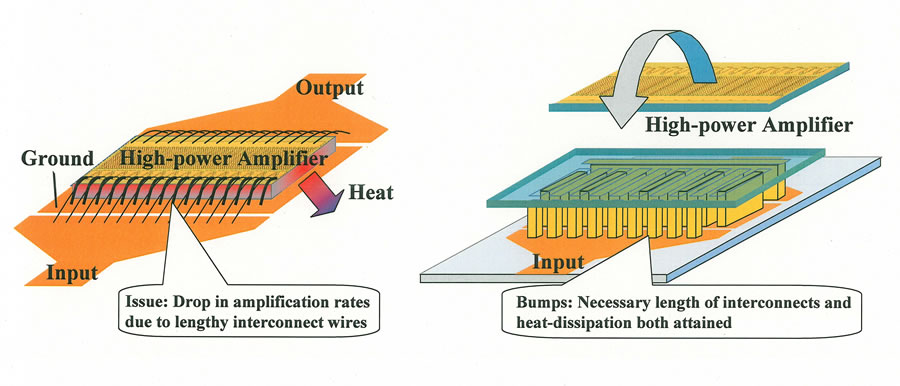
Two key technological issues for the realization of high-frequency, high-output amplifiers are the following: electrical interconnect methods needed to ensure that amplification rates do not drop at high frequencies, and heat-dissipation methods employed to control heat for high-power output. As conventional electrical interconnects use long metallic wires, at high frequencies the length of the wires causes the amplification rate to drop. Additionally, with conventional methods, making the transistor chips smaller does not allow for sufficient surface area (chip size) for heat-dissipation, which thereby made practical miniaturization of the transistors extremely challenging.
Newly-developed Technology
By employing a structure called a flip-chip structure (Figure 1) which features excellent high-frequency characteristics, Fujitsu Laboratories developed "dual-side heat-dissipation" technology in which heat is dissipated from both sides of the amplifier's transistor - the heat source - resulting in an amplifier that achieves high frequency, high output, and high amplification. This new technology makes possible the realization of high-frequency, high-output 100W-class amplifiers for 4G (IMT-Advanced) mobile communication systems.
 Figure 1: Conventional circuitry method, face-up structure (left) and flip-chip structure (right)
Larger View (68 KB)
Fujitsu's new dual-side heat-dissipation technology is realized by the following technologies:
1. Carbon nanotube-based heat-dissipation technology
Using the flip-chip structure, carbon nanotube bumps(3) were run between the electrode (metallic connectors) on the top of the amplifier (the circuitry surface) and the substrate, thereby increasing heat dissipation. In addition, a heat sink was affixed to the reverse side of the amplifier, so that heat is drawn away from the amplifier from both its front and back sides, thus further improving heat-dissipation (Figure 2).
 Figure 2: Dual-side heat-dissipation (on front and back of a high-power amplifier)
Larger View (50 KB)
2. Technology to grow carbon nanotubes
1. Carbon nanotubes grown to lengths of 20 µm (micrometers)(4) or longer (Figure 3)
If carbon nanotubes that are connected to the amplifier are too short, it will degrade electrical performance, making it difficult to attain high amplification rates. To attain high amplification rates at high frequencies, the interconnects need to be at least 10 µm long. By using an aluminum-iron (Al-Fe) film to grow carbon nanotubes to a length of 20 µm or longer perpendicular to the board, Fujitsu Laboratories achieved necessary interconnect length and high amplification rates.
2. Carbon nanotube bumps formed requiring electrode-mounting area of just 10µm or less (Figure 3)
To achieve high heat-dissipation, it is essential that carbon nanotube bumps be placed near the heat-source transistor of the amplifier. With conventional technology employing gold or solder bumps, it is impossible to make the bumps smaller than 20-25 µm, meaning that the bumps cannot be directly connected to the extremely miniature electrodes on the heat-source transistors. By employing technology that forms miniature carbon nanotube bumps of 10 µm or less, and by directly connecting the carbon nanotube bumps to electrodes, Fujitsu Laboratories realized excellent heat dissipation.
 Figure 3: Carbon nanotube bumps formed on electrodes Figure 3: Carbon nanotube bumps formed on electrodes
Larger View (11 KB) |
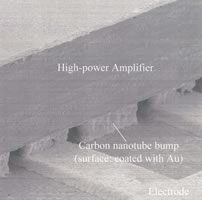 Figure 4: Carbon nanotube bump-based mounting of a high-power amplifier Figure 4: Carbon nanotube bump-based mounting of a high-power amplifier
Larger View (54 KB) |
Results
Fujitsu Laboratories' newly-developed "dual-side heat dissipation" technology enables 100W-class operation of flip-chip-mounted high-power amplifiers. The new technology improves heat-dissipation by an increase of 1.5 times compared to conventional methods. Furthermore, the technology makes it possible to reduce transistor chip size by approximately two-thirds (2/3) that of existing transistor chips, thus paving the way for amplifiers that are more compact.
Future Developments
Fujitsu Laboratories plans to continue with development of this technology targeting practical use in 100W-class amplifiers, and will strive for application of this technology for 4G (IMT-Advanced) mobile phone base stations which are anticipated to commence service from 2011.
-
[1] Carbon nanotubes
A tube made from a sheet of graphite (the same materials used in pencils) that has been wrapped into a cylinder. As its name implies, the diameter of a nanotube ranges from 1 to 10 nanometers, while its length is several thousand times longer than its diameter. Carbon nanotubes have superior physical properties, including tough mechanical strength, chemical stability, high thermal conductivity, low resistance, high aspect ratio, and high allowable current density.
-
[2] Flip-chip
A mounting method for mounting onto a board. Rather than the conventional method of connecting to a board via metallic wires, the chip's circuitry side is connected directly to protruding electrodes on the board.
-
[3] Bump
A protruding electrode formed on the surface of a semiconductor chip, used to connect semiconductors and boards. Materials used for bumps can be gold, solder, or carbon nanotubes.
-
[4] µm
Micrometer, 0.001mm.
About Fujitsu Laboratories
Founded in 1968 as a wholly owned subsidiary of Fujitsu Limited, Fujitsu Laboratories Limited is one of the premier research centers in the world. With a global network of laboratories in Japan, China, the United States and Europe, the organization conducts a wide range of basic and applied research in the areas of Multimedia, Personal Systems, Networks, Peripherals, Advanced Materials and Electronic Devices. For more information, please see:http://jp.fujitsu.com/group/labs/en/
Technical Contacts
Nanoelectronics Research Center
![]() Phone: +81(46)250-8234
Phone: +81(46)250-8234
![]() E-mail: nano-mate@labs.fujitsu.com
E-mail: nano-mate@labs.fujitsu.com
Company:Fujitsu Laboratories Ltd.
Company and organization names referenced herein are trademarks or registered trademarks of their respective owners. Information provided in this press release is accurate at time of issue and is subject to change without advance notice.
Date: 11 December, 2009
City: Kawasaki, Japan
Company:
Fujitsu Laboratories Ltd.,
,
,
,
,