![]()
Archived content
NOTE: this is an archived page and the content is likely to be out of date.
Fujitsu Laboratories Develops CMOS Transmitter IC for 40Gbps Optical Transmission Systems
- World's first 65nm standard CMOS-based single-chip integration of all functions necessary for 40Gbps transmitter ICs -
Fujitsu Laboratories Ltd.,Fujitsu Laboratories of America Inc.,Fujitsu Limited
Fujitsu Laboratories Limited, Fujitsu Laboratories of America, Inc., and Fujitsu Limited today announced the development of the world's first 65 nanometer (65nm) standard CMOS technology(1)-based transmitter IC (serializer) for 40 gigabits-per-second (40Gbps) trunk-line optical transmission systems. New circuit technologies were developed, for the realization of high-speed signal generation circuits capable of handling 40Gbps transmissions, in addition to enabling stable generation of 40Gbps output signals, within power voltage fluctuation ranges required for practical use. This is the first realization ever of a CMOS-based transmitter for optical transmission systems that integrates on a single chip the I/O interface(2), signal processing(3), and high-speed signal generation(4) that are all necessary for 40Gbps transmissions. As the first-ever single-chip integration of these multiple functions on a 40Gbps transmitter IC, this new transmitter IC will contribute significantly to the realization of power-efficient, low-cost, and compact optical transmission systems.
Details of these technologies were presented at the IEEE International Solid-State Circuits Conference 2009 (ISSCC 2009), held in San Francisco from February 8 to February 12 (Presentation 21.2).
Part of this research was conducted by the Optoelectronic Industry and Technology Development Association (OITDA) of Japan, under a contract from the New Energy and Industrial Technology Development Organization (NEDO) of Japan for its project, "Development of Next-generation High-efficiency Network Device Technology".
Background
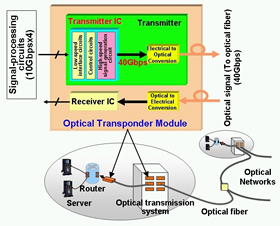 Figure 1: Block diagram of an optical transmission system
Larger View (234 KB)
To cope with the increasing volumes of data traffic concurrent with the widespread use of broadband networks, installation of optical transmission systems capable of 40Gbps high-speed transmissions on trunk-line networks is underway. In order to further spread the availability of 40Gbps optical transmission systems, there is a need for optical transmission relay equipment that is more power-efficient, smaller, and more affordable.
Optical transmitters require an IC that outputs a high-speed electrical signal of 40Gbps, by multiplexing together multiple electrical signals, each running at a relatively slow speed of 2.5Gbps to 10Gbps. Currently, transmitter ICs employ CMOS process technology for the low-speed interface circuitry and internal control circuitry, but require high-power compound semiconductors(5) for high-speed signal generator circuits that generate 40Gbps-electrical signals (Figure 1). If CMOS technology - which in accordance with miniaturization has become capable of high-speed operation - could be used for the signal-generating circuit, and if all required transmitter functions could be integrated onto a single chip by employing CMOS technology, optical transmission equipment that is power-efficient, compact, and low-cost can be realized.
Technological Challenges
In order to employ CMOS technology to enable high-speed operation in the signal-generating circuitry and to realize output of 40Gbps output waveforms at qualities equivalent to those generated by compound semiconductors, not only does the operational speeds of data-transmitting circuits need to be accelerated, but the clock signals - which are provided to circuits to determine their operational timing, must operate at 20GHz with low noise and sufficient amplitude. One major cause of amplitude degradation as the clock signals are distributed to the circuit is parasitic capacitance(6), from interconnects and elements. Due to the fact that CMOS has higher parasitic capacitance than compound semiconductors, in order to suppress amplitude degradation of clock signals at 20GHz, it is essential that the impact from parasitic capacitance be minimized. Furthermore, miniaturization of transistors as a means for higher performance also results in lowering of their breakdown voltage, thus limiting the usable power-supply voltage to a low 1V to 1.2 V. This means that a fluctuation in the power-supply could prevent sufficient voltage from reaching the circuit, thereby disrupting stable operation. Key challenges to reducing the cost of optical transmission systems under such fluctuating usage conditions have included the achievement of maintaining stable timing factors for the data signals and clock signals in circuits, and development of circuits that feature stable operation.
Newly Developed Technology
Fujitsu Laboratories have developed the technologies below, which have resulted in the world's first transmitter IC that features 40Gbps high-speed performance while generating a stable 40Gbps output signal across the range of temperature and voltage conditions that are required for commercial use.
1. Clock-signal distribution technology
A new circuit technology was developed for the clock-distribution circuit in the transmitter IC, with which loss of clock signal swing is compensated by using inductors(7) and low-power distribution of a low-noise clock signal becomes possible. Conventionally, to minimize the effects of parasitic capacitance, compensation using inductors to cancel capacitance have been used. By focusing on the fact that clock signals in the transmitter IC use a single frequency, new high-speed technology was used in which the inductor compensates for the parasitic capacitance only in the frequency band around the signal frequency, thereby enabling low-noise, high-speed transmission of clock signals, with fewer circuit stages.
2. Automatic timing-adjustment technology
A new circuit technology has been applied to the output circuit, with which timing of the clock signal – which controls circuit operation – and the data signal which passes through the circuit is continually monitored in order to optimize the relationship between the two signals. In this circuit technology, the monitoring and adjusting mechanisms are segregated from the data-signal transmission pathway, so that additional circuits needed to implement these mechanisms do not degrade the data-signal waveform, while allowing for the timing of the two signals to be automatically coordinated to realize fast data signal transmissions with stable waveforms.
Results
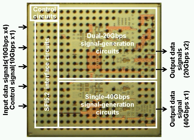
 Figure 2: Photo of the new transmitter IC
Larger View (364 KB)
By applying the aforementioned technologies to the design of a CMOS-based signal-generating circuit and by integrating the low-speed interface circuit and control circuits, Fujitsu Laboratories has succeeded in the development of the world's first single-chip 65nm standard CMOS-based transmitter IC (Figure 2).
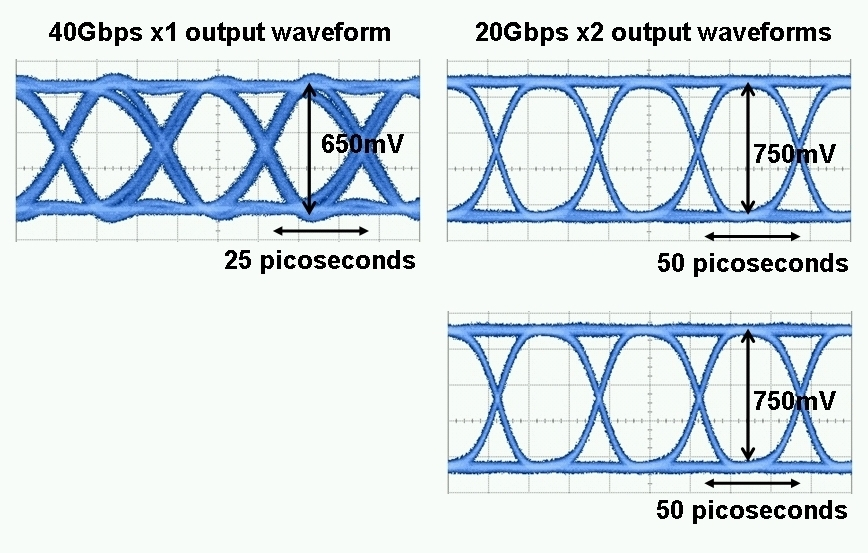
As illustrated in Figure 3, the output waveform of the IC implementing the newly-developed technologies is stable and sharp, and has been verified by Fujitsu Laboratories to produce a reliable 40Gbps data output signal (data error rate less than 10-12, less than one error per trillion bits) over a commercial temperature and voltage variation range. These technologies have also been verified as being effective for fluctuations in operating temperature, in addition to effectiveness for power voltage fluctuations.
 Figure 3: Output waveform measurements of the new transmitter IC (y axis: output voltage, x axis: time)
Larger View (306 KB)
One-chip integration and new clock-distribution circuitry permit power consumption to be lowered to less than 2W, one-third (1/3) that of conventional transmitter ICs. Since low-power operation reduces heat generation, it permits higher-density mounting of optical transceiver modules in optical transmission equipment. Compared to conventional 40Gbps equipment new transponders made using this technology will be roughly half the size, resulting in lower overall cost.
This transmitter IC is the first ever to use the SFI5.2(8) interface, which has emerged as a standard in recent years for low-speed interfaces. By taking advantage of high-integration capabilities available in CMOS technology, the transmitter IC also has ability to output two 20Gbps signals in order to support a signal modulation technique intended for long-distance transmissions (Figure 3). This CMOS-based transmitter IC makes it possible for multiple systems to be handled by single chip, which is anticipated to lead to widespread availability of 40Gbps optical transmission equipment.
Future Developments
Fujitsu Laboratories will continue to further refine the 40Gbps output waveform of this new transmitter IC. The company will also continue with advances for development of a CMOS-based receiver IC, to contribute to reduction of optical transmission equipment. The developments results for the new transmitter IC will be applied not only to trunk-line optical transmission systems, but also in the future to 40G Ethernet serial optical devices, to enable faster-operation LANs and corporate networks.
For more information:
-
[1] CMOS technology
A semiconductor technology comprised of N-type and P-type metal-oxide semiconductor (MOS) transistors with complementary connections, created on a silicon substrate. Attributable to their low power requirements, CMOS integrated circuits are currently the mainstream.
-
[2] I/O interface (Input/Output interface)
Refers to functions for I/O signal logic and sequencing, and transmitter IC operation mode, which can be controlled using I2C bus interface.
-
[3] Signal processing
Refers to the following functions: a data-recovery function that enables five 10Gbps electrical signals to be received without error, a function that accommodates timing errors between these five signals, and a function that synchronizes the timing of these signals.
-
[4] High-speed signal generation
A function that receives four 10Gbps electrical signals, and generates either two 20Gbps electrical signals or one 40Gbps electrical signal.
-
[5] Compound semiconductor
A semiconductor formed using two or more elements, such as gallium-arsenide (GaAs) or indium-phosphide (InP), and which features higher electron mobility than silicon, therefore permitting faster operation.
-
[6] Parasitic capacitance
Undesirable static capacitance that emerges between a transistor element's Input/Output (I/O) electrodes, or between the transistor and electrodes of peripheral elements surrounding the transistor. The amount of parasitic capacitance varies depending on the electrode size of the elements or distance between elements, thus making it impossible to indicate parasitic capacitance in schematic circuit diagrams.
-
[7] Inductor
A coil element in which electrical conductivity becomes more difficult at higher frequencies (passes low-frequency signals, but resists passage of high-frequency signals). Inductors are usually formed as coil circuit patterns on semiconductors.
-
[8] SFI5.2
Serdes Framer Interface Level 5 Phase 2. Refers to a standard promulgated in October 2006 at the Optical Internetworking Forum (OIF) 2006.
About Fujitsu Laboratories
Founded in 1968 as a wholly owned subsidiary of Fujitsu Limited, Fujitsu Laboratories Limited is one of the premier research centers in the world. With a global network of laboratories in Japan, China, the United States and Europe, the organization conducts a wide range of basic and applied research in the areas of Multimedia, Personal Systems, Networks, Peripherals, Advanced Materials and Electronic Devices. For more information, please see:http://jp.fujitsu.com/group/labs/en/
About Fujitsu Laboratories of America, Inc.
Fujitsu Laboratories of America, Inc. is a wholly owned subsidiary of Fujitsu Laboratories Ltd. (Japan), focusing on research on advanced VLSI CAD, Internet, and interconnect technologies. Conducting research in an open environment, it contributes to the global research community and the working IT industry. It is headquartered in Sunnyvale, CA.
For more information, please see: www.fla.fujitsu.com
About Fujitsu
Fujitsu is a leading provider of IT-based business solutions for the global marketplace. With approximately 160,000 employees supporting customers in 70 countries, Fujitsu combines a worldwide corps of systems and services experts with highly reliable computing and communications products and advanced microelectronics to deliver added value to customers. Headquartered in Tokyo, Fujitsu Limited (TSE:6702) reported consolidated revenues of 5.3 trillion yen (US$53 billion) for the fiscal year ended March 31, 2008. For more information, please see: www.fujitsu.com.
Technical Contacts
Network SOC Development Lab.System LSI Development Lab.
![]() Phone: +81(44)754-2692
Phone: +81(44)754-2692
![]() E-mail: 40g_pr@ml.labs.fujitsu.com
E-mail: 40g_pr@ml.labs.fujitsu.com
Company:Fujitsu Laboratories Limited
Company and product names referenced herein are trademarks or registered trademarks of their respective owners. Information provided in this press release is accurate at time of issue and is subject to change without advance notice.
Date: 13 February, 2009
City: Kawasaki and Tokyo, Japan and Sunnyvale, U.S.
Company:
Fujitsu Laboratories Ltd.,
Fujitsu Laboratories of America, Inc.,
Fujitsu Limited,
,
,