![]()
Archived content
NOTE: this is an archived page and the content is likely to be out of date.
Fujitsu Develops High-Speed, Power-Efficient ReRAM Featuring Limited Fluctuation of Resistance Value
Fujitsu Laboratories Ltd.
Fujitsu Laboratories Ltd. today announced the development of a new type of resistive RAM(ReRAM)(1), a type of non-volatile memory(2), which combines low power consumption with limited fluctuation of resistance value. By changing the structure of the ReRAM by adding titanium (Ti) to nickel oxide (NiO), and by limiting the current flow from the transistor, Fujitsu Labs has successfully reduced the current needed to erase memory to 100 micro-amperes or less. Furthermore, even in high-speed erasure operations requiring only 5 nanoseconds, fluctuation of resistance value which affects the device's quality has been reduced to one-tenth (1/10th) that of conventional ReRAMs. Fujitsu Labs views the new ReRAM as an alternative to flash memory that combines high speed and low power consumption, in a low-cost embedded memory(3).
Details of this technology were presented at the IEDM (International Electron Devices Meeting), held from December 10-12 in Washington, D.C. (Session: 30.1).
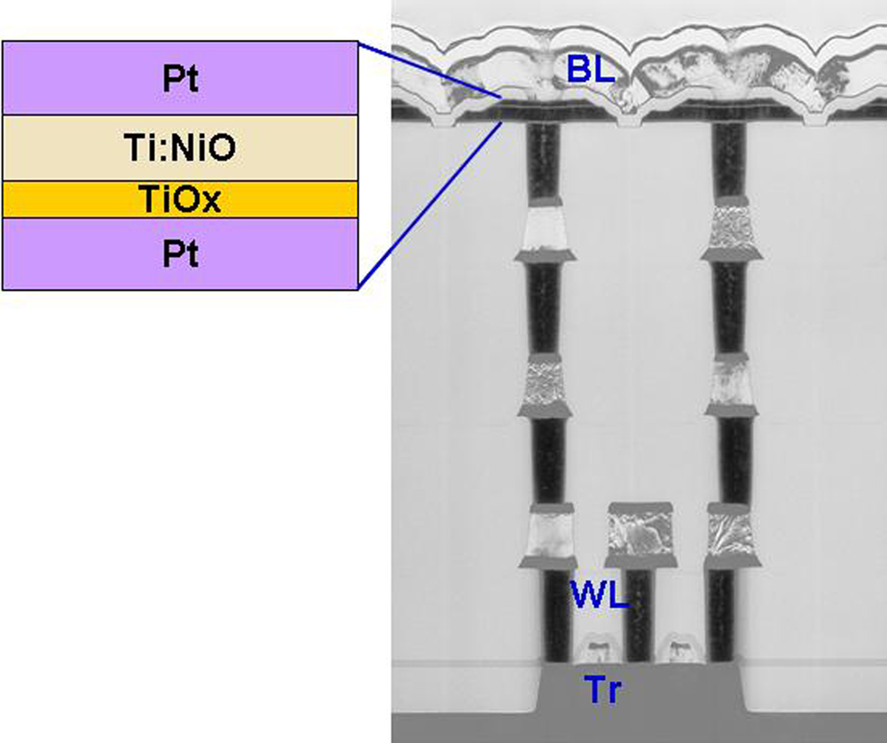
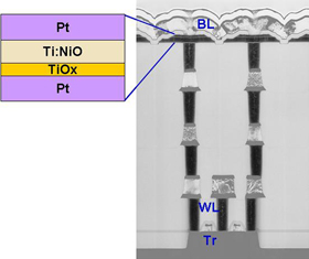 Figure 1: Fujitsu Labs' newly developed ReRAM device (left) in combination with a transistor (right)
Larger View (205 KB)
Background
As with flash memory microcontrollers, current system LSIs feature embedded non-volatile memory- such as flash memory - rather than read-only memory (ROM). These system LSIs which enable software to be updated after manufacture are becoming the mainstream. However, it is anticipated that miniaturization of flash memory will reach its limits in the near future, and a number of memory technologies are under development as alternatives to flash memory.
ReRAM is a type of memory that uses material for which the resistance value changes when voltage is applied. ReRAM is amenable to miniaturization and can be manufactured inexpensively, making it attractive as an alternative to flash memory.
Technological Challenges
An important issue in the development of ReRAM has been the reduction of current required to erase memory. Also, when subjected to repeated, high-speed write and erase operations, ReRAM's resistance value tends to fluctuate, which is known to impair device quality. As such, controlling fluctuation of resistance value is of great importance for ReRAM.
Newly Developed Technology
Conventionally, ReRAM devices have been formed from nickel oxide (NiO) films. In Fujitsu Labs' new ReRAM, a NiO film doped with titanium (Ti:NiO) was developed, and its performance was evaluated in combination with a transistor (see Figure 1).
As a result, voltage can be increased for memory erasures, and operations require only 5ns, approximately 10,000 times faster than in the past. At the same time, fluctuations in resistance value have been reduced to one-tenth (1/10th). Furthermore, by optimizing the voltage applied to the transistor, current required for an erase operation is reduced to 100 micro-amperes or less.
Results
By utilizing this new material, Fujitsu Labs created a prototype ReRAM device that features low fluctuation of resistance value, even during high-speed operation.
As an alternative to flash memory, if further minute non-volatile memory can be realized using ReRAM, there is potential for higher performance of mobile devices.
Future Developments
Fujitsu Labs plans to conduct further R&D related to ReRAM, such as development of miniaturization process technologies for ReRAM devices, and design of read and write circuits.
For more information:
-
[1] ReRAM
Resistive Random Access Memory. Memory that makes use of enormous resistive changes in the memory device, in the presence of an electrical field.
-
[2] Non-volatile memory
Memory that retains data even after power is turned off.
-
[3] Embedded memory
Memory that is embedded into a system LSI.
About Fujitsu Laboratories
Founded in 1968 as a wholly owned subsidiary of Fujitsu Limited, Fujitsu Laboratories Limited is one of the premier research centers in the world. With a global network of laboratories in Japan, China, the United States and Europe, the organization conducts a wide range of basic and applied research in the areas of Multimedia, Personal Systems, Networks, Peripherals, Advanced Materials and Electronic Devices. For more information, please see:http://jp.fujitsu.com/group/labs/en/
Technical Contacts
Embedded Memories Development Dept.Silicon Technologies Development Lab.
![]() Phone: +81-46-250-8379
Phone: +81-46-250-8379
![]() E-mail: emd-si@ml.labs.fujitsu.com
E-mail: emd-si@ml.labs.fujitsu.com
Company:Fujitsu Laboratories Ltd.
All company or product names mentioned herein are trademarks or registered trademarks of their respective owners. Information provided in this press release is accurate at time of publication and is subject to change without advance notice.
Date: 14 December, 2007
City: Kawasaki, Japan
Company:
Fujitsu Laboratories Ltd.,
,
,
,
,